Continue to Site

Welcome to EDAboard.com

Welcome to our site! EDAboard.com is an international Electronics Discussion Forum focused on EDA software, circuits, schematics, books, theory, papers, asic, pld, 8051, DSP, Network, RF, Analog Design, PCB, Service Manuals... and a whole lot more! To participate you need to register. Registration is free. Click here to register now.

how to realize 3.3v to 1.2v(can't use LDO. if DC-DC,then shouldn't use inductor)

Status
Not open for further replies.
I have managed to find my mistake in my unworkable method of pulsing current to the load and smoothing capacitor combined.

For a while I did not see a breakdown in efficiency between step 1 and 2:
(Step 1) A raw switch-on-switch-off configuration (95% efficient), and
(Step 2) the idea of adding a capacitor to smooth pulses.

I had to resort to my simulator. It showed me my mistake. It was not with the help of math or by theoretical axioms.

A solution to the OP should not care about a capacitor being (or not being) in the power supply. No need to calculate the decline in energy when a charge is distributed to a second capacitor. I used an ideal power supply. Zero ohms, no droop under load, no ripple. 3.3 V.

I discovered that the inefficiency enters in because the capacitor draws extreme current as it tries to charge to the full 3.3V while the pulse is on.

I tried the simulation with a small capacitor. A small cap reaches 3.3 V quickly. Then the pulse shuts off, and the cap discharges through the load quickly. This won't work. This is what I anticipated in the case of a small cap.

I tried a large cap. It charges a little higher with each pulse. The rate depends on the transistor's minimum 'on' resistance. I used 1 ohm. This makes resistive reduction a minor factor. I discovered a large capacitor does not end up settling at a charge of 1.2V to reflect a duty cycle of 35 percent (even though I thought it should). It seeks to reach 3.3 V, drawing extreme current during each pulse.

So now a couple of things are unsettling me:

* Finding my assertions were incorrect after I'd stated them confidently to those more knowledgeable than me,

* finding that a concept which is so good that it really ought to work, doesn't. Not with the efficiency it looked like it ought to have.
 

hi,all
now i need convert 3.3v or 2.5v to 1.2v~1v in cmos0.13um process. if i can't use LDO, only use DC-DC(but without inductor!).how can i do? the ripple need to keep below 50mv.loding up to 30mA .and efficiency > 60~70% is accepted.
Does anyone has relate experience,or some proble way? i need you help, idea, reference papers,or any relate note.


with LDO efficiency is vout/vin so you can realize LDO with 34% efficiency
w/o inductors you need two external caps to realize switched capacitor basec charge pump

single cap solution presented by Brad is great but there are switching loss Cv^2F across the bipolar and IR loss
 

Thanks for your replys!

BradtheRad,
Let's simply calculate, as pnp switch "on" in DT, "off" in (1-D)T,then when system is stable, (Iin-Iout)*DT=Iout(1-D)T--->IinD=Iout;
thus max of η=Pout/Pin=Vout*Iout/(Vin*IinD)=Vout/Vin; so just with this kind of SC capacitors ,we may couldn't get η>Vout/Vin; just as LvW conculated before; here also i confused how (vin-vout)/vin waste?
since switch with pwd of SC capacitors is not useful as η < LDO. maybe we only could use charge pump convertors.
So, my doubt become as follow:
1, if big extra capacitors outside is allowed, then how we can realize 2.5v-->1.2v while meeting ripple&η.
2, if use charge pump convertors, is the principles keep capacitors delta V constant(or means Q constant).and if it is,how can i realize vout adjustment as:1.0v,1.1v,1.2v.
3,who can give me some relate papers use this method?

Thanks and Happy new Year!
 

BradtheRad,
Let's simply calculate, as pnp switch "on" in DT, "off" in (1-D)T,then when system is stable, (Iin-Iout)*DT=Iout(1-D)T--->IinD=Iout;
thus max of η=Pout/Pin=Vout*Iout/(Vin*IinD)=Vout/Vin; so just with this kind of SC capacitors ,we may couldn't get η>Vout/Vin; just as LvW conculated before; here also i confused how (vin-vout)/vin waste?
since switch with pwd of SC capacitors is not useful as η < LDO. maybe we only could use charge pump convertors.
So, my doubt become as follow:
1, if big extra capacitors outside is allowed, then how we can realize 2.5v-->1.2v while meeting ripple&η.
2, if use charge pump convertors, is the principles keep capacitors delta V constant(or means Q constant).and if it is,how can i realize vout adjustment as:1.0v,1.1v,1.2v.

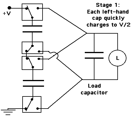
At this point it's helpful to have diagrams showing the method which has been held up as the ideal. Theoretically this method is 100 percent efficient.

Stage 1 (The left-hand capacitors should be equal, so that they charge at the same rate):

15_1325671863.gif


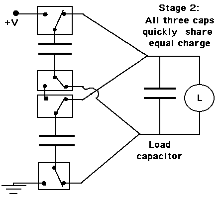
Stage 2:

40_1325671863.gif


We can adjust duty cycle, switch rate, and capacitor values, in order to bring ripple within spec.

One thing not shown in the schematics is the impedance in the power supply. It has a lot to do with how fast the left-hand capacitors charge.

We have divided the supply by 2. But suppose net voltage to the load is slightly high? It can be reduced by putting a resistor or two somewhere in the loop. It will dissipate some power, reducing efficiency somewhat.

Suppose we want V/3? Then we stack 3 capacitors at the left. It will require adding more switches. (The switches are single-pole double-throw type.) No efficiency is lost. Using this process we can divide down to whatever level we wish.

Switches are inconvenient. To make a working project, we would like to replace all switches with mosfets. The hard part is figuring out how to do it yourself. It will require a lot of devices, because it takes 2 mosfets to do the job of 1 double-throw switch.

Furthermore each mosfet's gate voltage is referenced to the source terminal (n-mos) or drain terminal (p-mos). However the proper voltage may or may not be present at the proper terminal. Or it may not be sufficient. This brings in the likelihood that we need to step up voltages at gates, or use pulse transformers, etc.

What if we tried to use transistors? We would run into a similar problem. Bias currents would not necessarily have a clear path to ground (or to positive polarity in the case of PNP type). This stops transistors from operating properly.

So the project has become quite complex.

It's easier to use a simpler linear (voltage drop) step down configuration. Despite their wasting more power.

If an inductor is allowed, then greater efficiency is possible.
 

Thanks RobG.
It's nice OP when used as voltage double,
but how could i converte it into step down mode?such as 1/2 with GmV modulation for Vout? i can't work out....


---------- Post added at 03:37 ---------- Previous post was at 03:26 ----------

BradtheRad,
i couldn't understand how it go into stable system with constant load current Iout....
thought stage2 left cap=Cin ,load cap=CL,then 2Cin*vbat/2=(2Cin+CL)Vo--->Vo<vbat/2(when CL~0),if it's ,how system work in stage 1 while Iout bring Q out.
could you pls show me some fomular as stage1-->stage2--->stage1. should load capacitor all floating in stage 1 or it's bottom always to gnd ?
 

The load capacitor is needed to drive the load while the left-hand caps are charging.

Cycles alternate rapidly between Stages 1 and 2. After a few cycles the load cap will rise close to V/2.

The bottom switch can be removed, and the 3 wires can be joined into one node at ground.

While the method of switching capacitors appeared to be the ideal solution, it also has its own problems. For one, there are large current surges. Any device used to switch the capacitors must handle high current.

On the other hand, if only small current is required, then the method in post #25 is going to a lot of trouble.

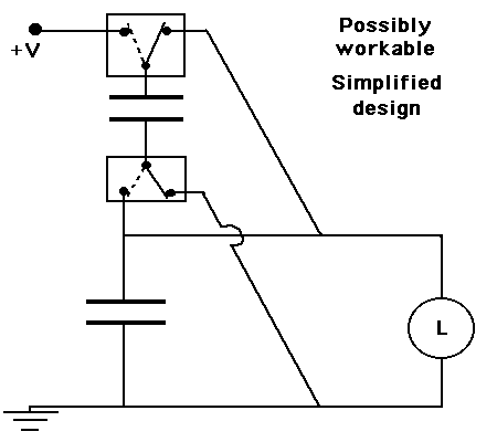
I condensed the design of post #25 into a simpler version. After simulating it I find that it has a chance of working if a load voltage of 1.5 is not too high.

78_1325771442.gif


The switches shall be replaced by the proper network of mosfets/transistors. This will be a job in itself.

The capacitors need to be a few hundred uF. This is to prevent sudden current spikes that create large ripple fluctuations at the load.

Some resistors can be added to reduce the spikes, but it will also reduce efficiency.
 
Last edited:

Thanks RobG.
It's nice OP when used as voltage double,
but how could i converte it into step down mode?such as 1/2 with GmV modulation for Vout? i can't work out....

I was thinking that the derivations used there might be helpful to the OP and show the upper limits of efficiency and how to find stability, output impedance, etc. They also apply to step down charge pumps, so hopefully he/you can figure out how they can be adapted. This is the only paper I know of that covers most of the basics. When I wrote it I couldn't find any overview papers to reference, but I could have missed it.

I'd use a 1:2 cap divides to generate Vdd/2 like we've been talking about and a regulator to bring it to 1.2V.

rg
 

I think with switching you can attain the required out put. and you may not be needing any inductance for the process.
 

Status
Not open for further replies.

Part and Inventory Search

Welcome to EDABoard.com

Sponsor

Back
Top