by Bill Schweber on Analog IC Tips
We have already looked briefly at Earth ground (if any), chassis ground, and commons (often misnamed as "grounds"). These do not exist as unrelated connections in a system. The issues related to connecting commons and ground is the subject of countless articles, academic papers, vendor application notes, anecdotes, and even books.
There are many rules as to how to connect circuit commons to each other, to the chassis ground (if there is one) and to the Earth ground (again, if there is one). Each of these rules has many legitimate exceptions which means the final decision is determined by regulatory requirements, good engineering practice, and performance goals.
What’s the relationship between the schematic diagram and the physical connections?
There is little relationship. The schematic shows the physical connections but not the layout or actual configuration. It shows what you would get if you checked connections with a continuity tester. For grounds and commons, though, much of the story is how and where they are connected to each other, by what means, over what distance, and more. The schematic shows little or none of this information.
What is a key difference between a schematic diagram's ground/common topology and the real-world implementation?
In principle, a ground or common is an equipotential plane, and it has zero DC resistance and AC impedance when measured between any two points. In the real world, there will always be some impedance between two points, current flow, and a resultant voltage drop. Remember, the more-accurate term for what we call “voltage” is really “potential difference” and it only has meaning between two defined points. Whenever there is current flow and voltage drop, the ground/common is no longer idea. Therefore, the real-world paths of wires, PC board traces, and board areas will only approximate an ideal zero-resistance plane.
Also keep in mind that any currents flowing in a ground or common can from somewhere and go to somewhere, they do not exist in a circuit "vacuum". A ground or common is part of the return path for current flowing from the power source and rails, through the circuit, and back to the power source. So the issues are to note are "from where is the ground current coming?", and "where is it going?"
How are common points and their paths usually connected?
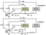
In general, all analog-circuit commons should be connected together, but at only one point, in what is called a "star" topology, Figure 1; similarly, the digital-circuit commons are usually also connected to this unique point. The challenge for the designer and layout is to establish the path by which each of these commons reaches the star point. The paths need to be short, direct, and independent of the other paths. In general, grounds and common paths should not run parallel to each other, as they may induce cross currents.

Fig 1: Digital currents flowing in analog return path create error voltages. (from Analog Devices)
Should ground and commons points always be connected?
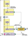
Again, the guidelines about connecting ground and commons are only guidelines, not absolute. While the answer is generally “yes”, there are many important exceptions. For example, when using an electrically isolated circuit to measure the voltage across the top battery in a stack, Figure 2, it is essential that the common of the measurement front end and the common of the rest of the circuitry – whether grounded or not – not be connected to each other, as doing so would completely defeat the critical isolation.

Fig 2: Monitoring the analog voltage of a single battery at the top of a series stack of batteries requires careful attention to grounds and safety; in most cases, isolation of the battery-side front end from the rest of the system in mandated, so any connection between their two "common" points is not allowed. (from Analog Devices)
What is a ground loop?
Whenever there is a potential difference between two ends of a ground/common path, or between two ground/common points which are connected together, the resultant current flow and voltage is what is called a ground loop. In general, ground loops can cause problems because this flow of current is contrary to the needs of a good ground/common environment. In many cases, lower-impedance connections or even isolator circuits (with no ohmic/galvanic path between the two points) which are used to minimize or even break ground loops.
What about AC line-powered systems?
This need for connecting commons and grounds in many (but not all) designs applies to AC-powered systems as well. While connecting the AC ground to chassis ground and the various commons is the normal practice and often mandatory, there are many cases where the AC ground must be kept separate (medical systems, for example, due to concerns about tiny leakage currents and patient safety). This AC isolation is usually implemented by using a transformer between the two sections.
How is a final determination made of the "best" or "right" way to connect ground and commons?
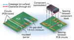
If AC line or higher voltages/currents are involved, the topology starts with regulatory and safety mandates for topology and physical implementation, including key dimension parameters such as creepage and clearance, Figure 3. Many engineers proceed using the generally suggested guidelines, while also keeping in mind the conflicting demands that these posed when used in conjunction with other circuit and system constraints. Also, these guidelines may actually contradict each other, depending on the author's application and personal experience.\

Fig 3: The definition and minimum dimensions for creepage and clearance requirements are a function of working voltage, and are defined by various regulatory and safety agencies. (from PCB Design Tech Guide)
Using or at least starting with a verified, tested reference design with detailed layout files is a step that many engineers also consider, so they can at least see what another design team has successfully accomplished. The reality is that takes both science and art, as well as experience and knowledge of regulatory requirements, to decide and conclude what to connect where — somewhat due to the uncertainty about where current will flow as dictated by Maxwell's equations.
References
(There are countless quality references of all lengths and technical levels; these are just a few.)
"Staying Well Grounded" (Analog Devices)
AN-42036, "PCB Grounding System and FAN2001/FAN2011 High Performance DC-DC Converters" (Fairchild/ON Semiconductor)
Application Note 1681, "Grounding Techniques" (Intersil Corp.)
"Isolation in High-Voltage Battery Monitoring for Transportation Applications" (Analog Devices)
We have already looked briefly at Earth ground (if any), chassis ground, and commons (often misnamed as "grounds"). These do not exist as unrelated connections in a system. The issues related to connecting commons and ground is the subject of countless articles, academic papers, vendor application notes, anecdotes, and even books.
There are many rules as to how to connect circuit commons to each other, to the chassis ground (if there is one) and to the Earth ground (again, if there is one). Each of these rules has many legitimate exceptions which means the final decision is determined by regulatory requirements, good engineering practice, and performance goals.
What’s the relationship between the schematic diagram and the physical connections?
There is little relationship. The schematic shows the physical connections but not the layout or actual configuration. It shows what you would get if you checked connections with a continuity tester. For grounds and commons, though, much of the story is how and where they are connected to each other, by what means, over what distance, and more. The schematic shows little or none of this information.
What is a key difference between a schematic diagram's ground/common topology and the real-world implementation?
In principle, a ground or common is an equipotential plane, and it has zero DC resistance and AC impedance when measured between any two points. In the real world, there will always be some impedance between two points, current flow, and a resultant voltage drop. Remember, the more-accurate term for what we call “voltage” is really “potential difference” and it only has meaning between two defined points. Whenever there is current flow and voltage drop, the ground/common is no longer idea. Therefore, the real-world paths of wires, PC board traces, and board areas will only approximate an ideal zero-resistance plane.
Also keep in mind that any currents flowing in a ground or common can from somewhere and go to somewhere, they do not exist in a circuit "vacuum". A ground or common is part of the return path for current flowing from the power source and rails, through the circuit, and back to the power source. So the issues are to note are "from where is the ground current coming?", and "where is it going?"
How are common points and their paths usually connected?
In general, all analog-circuit commons should be connected together, but at only one point, in what is called a "star" topology, Figure 1; similarly, the digital-circuit commons are usually also connected to this unique point. The challenge for the designer and layout is to establish the path by which each of these commons reaches the star point. The paths need to be short, direct, and independent of the other paths. In general, grounds and common paths should not run parallel to each other, as they may induce cross currents.
Fig 1: Digital currents flowing in analog return path create error voltages. (from Analog Devices)
Should ground and commons points always be connected?
Again, the guidelines about connecting ground and commons are only guidelines, not absolute. While the answer is generally “yes”, there are many important exceptions. For example, when using an electrically isolated circuit to measure the voltage across the top battery in a stack, Figure 2, it is essential that the common of the measurement front end and the common of the rest of the circuitry – whether grounded or not – not be connected to each other, as doing so would completely defeat the critical isolation.
Fig 2: Monitoring the analog voltage of a single battery at the top of a series stack of batteries requires careful attention to grounds and safety; in most cases, isolation of the battery-side front end from the rest of the system in mandated, so any connection between their two "common" points is not allowed. (from Analog Devices)
What is a ground loop?
Whenever there is a potential difference between two ends of a ground/common path, or between two ground/common points which are connected together, the resultant current flow and voltage is what is called a ground loop. In general, ground loops can cause problems because this flow of current is contrary to the needs of a good ground/common environment. In many cases, lower-impedance connections or even isolator circuits (with no ohmic/galvanic path between the two points) which are used to minimize or even break ground loops.
What about AC line-powered systems?
This need for connecting commons and grounds in many (but not all) designs applies to AC-powered systems as well. While connecting the AC ground to chassis ground and the various commons is the normal practice and often mandatory, there are many cases where the AC ground must be kept separate (medical systems, for example, due to concerns about tiny leakage currents and patient safety). This AC isolation is usually implemented by using a transformer between the two sections.
How is a final determination made of the "best" or "right" way to connect ground and commons?
If AC line or higher voltages/currents are involved, the topology starts with regulatory and safety mandates for topology and physical implementation, including key dimension parameters such as creepage and clearance, Figure 3. Many engineers proceed using the generally suggested guidelines, while also keeping in mind the conflicting demands that these posed when used in conjunction with other circuit and system constraints. Also, these guidelines may actually contradict each other, depending on the author's application and personal experience.\
Fig 3: The definition and minimum dimensions for creepage and clearance requirements are a function of working voltage, and are defined by various regulatory and safety agencies. (from PCB Design Tech Guide)
Using or at least starting with a verified, tested reference design with detailed layout files is a step that many engineers also consider, so they can at least see what another design team has successfully accomplished. The reality is that takes both science and art, as well as experience and knowledge of regulatory requirements, to decide and conclude what to connect where — somewhat due to the uncertainty about where current will flow as dictated by Maxwell's equations.
References
(There are countless quality references of all lengths and technical levels; these are just a few.)
"Staying Well Grounded" (Analog Devices)
AN-42036, "PCB Grounding System and FAN2001/FAN2011 High Performance DC-DC Converters" (Fairchild/ON Semiconductor)
Application Note 1681, "Grounding Techniques" (Intersil Corp.)
"Isolation in High-Voltage Battery Monitoring for Transportation Applications" (Analog Devices)