userx2
Full Member level 3
Hello,
I am just designing the power circuit for a 24bit ADC chip interfacing to a microcontroller on the same PCB.
The manufacturer recommends separate regulators for the digital and analogue side. Fair enough.
But I am confused about the grounding configuration.
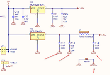
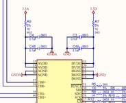
I thought the output caps of the analogue (3.3A) regulator should go to AGND but in this circuit, they have connected then to the Digital GND.
The ADC chip AGND pins and local decoupling caps are the only parts connected to the AGND.
Is that correct and what would be the reasoning behind that configuration?
Please see picture
Best regards
X
I am just designing the power circuit for a 24bit ADC chip interfacing to a microcontroller on the same PCB.
The manufacturer recommends separate regulators for the digital and analogue side. Fair enough.
But I am confused about the grounding configuration.
I thought the output caps of the analogue (3.3A) regulator should go to AGND but in this circuit, they have connected then to the Digital GND.
The ADC chip AGND pins and local decoupling caps are the only parts connected to the AGND.
Is that correct and what would be the reasoning behind that configuration?
Please see picture
Best regards
X