ivan_mateo
Member level 1
Hi everyone,
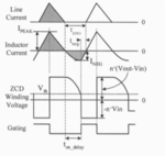
I am plannig to design a constant on time and vary frequency pfc circuit. I found some equations but could not understand how to zvvs is achived in that circuit. ınductor current ramp up at on time, and when the inductor current is decreased at off time. But off time is continue because current is negative and ton is delayed. Can anybody expalin how these theory expain with below equations?


I am plannig to design a constant on time and vary frequency pfc circuit. I found some equations but could not understand how to zvvs is achived in that circuit. ınductor current ramp up at on time, and when the inductor current is decreased at off time. But off time is continue because current is negative and ton is delayed. Can anybody expalin how these theory expain with below equations?