Continue to Site

Welcome to EDAboard.com

Welcome to our site! EDAboard.com is an international Electronics Discussion Forum focused on EDA software, circuits, schematics, books, theory, papers, asic, pld, 8051, DSP, Network, RF, Analog Design, PCB, Service Manuals... and a whole lot more! To participate you need to register. Registration is free. Click here to register now.

zero voltage switching class d h bridge

Status
Not open for further replies.

franticEB

Full Member level 3
Joined
May 10, 2010
Messages
152
Helped
1
Reputation
2
Reaction score
2
Trophy points
1,298
Activity points
2,540
Hi,
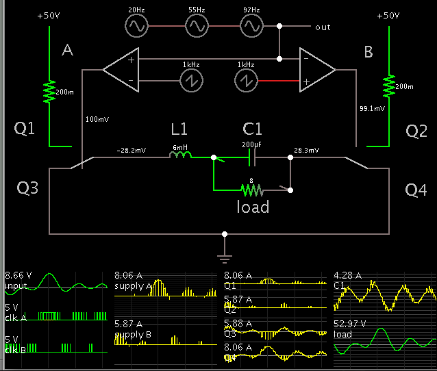
i'm designing and realizing on prototype board a full bridge class D amplifier.
The switching losses of mosfets are higher than those provided by the calculations.
The DC voltage is 250V and Fswitching=50KHz Pout=150Wrms.

My question is: is there in literature a ZVS class d amplifier example? Is it possible to realize it?
If yes is there any tutorial or application from which start the design?

If not could you suggest me a suitable kind of mosfet to be used, tutorial or handbook on that kind of amplifer?

Thanks a lot...
 

Harris electronics had a design tutorial on a dvd or a cd on digital sub-woofer design. I built a sub-woofer for my home theater from it. It really rocked the house! My son has it now. My wife would not let run it anymore.
If I can find the dvd/cd and Harris doesn't have it any more I'll ask for permission to copy it.
 

I'm really interested... keep me updated thank
 

class d mosfet too much dissipation

Hi,
i'm designing and realizing on prototypal board the class d amplifier in figure below

hbridge100w.jpg

the problem is that the Infineon MOSFETS become too hot beyond the calculations that I made, also without load and with lower voltage than i need. Also they present 100ns of miller plateau at which the measured current on high side mosfet drain is of any amperes.

I test many mosfets and they all have the same problem maybe less pronounced.

The only one that doesn't have that kind of dissipation issue is International Rectifier mosfet in figure.

What do you think? Is it a bad driving or parasitic components of other mosfets?

I'm looking for a mosfet with lower Rds in order to increase output power...
Could you help me?
Thanks
 

Re: class d mosfet too much dissipation

You didn't report any results (e.g. calculated versus measured losses), so I can just guess that you understimated the losses caused by charging the MOSFET output capacitances.

I presume you have varied deadtime to verify that it's not a cross-conduction problem.
 

Re: class d mosfet too much dissipation

The fact that i don't understand is that the infineon mosfets dissipate about 1.5W with no load and 70Vdc (instead of 250v).
I don't test the infinon mosfets with higher voltage or increasing load because of dissipation.
I calculate conductive and switching losses and if you compare the datasheets of indineon and irf infineon is better for Qgs Qgd Coss and Rds.
The only parameter on which i have difficulties in losses estimation is the Qrr. How can relate the datasheet value to my case?

I'm sure that it is not a cross condution problem.

The switching frequency is 50khz.
 

As said, you're reporting unloaded operation conditions. With or without out LC circuit? 1.5W each transistor, half-bridge or the complete full-brige? Did you check if switching losses vary with gate resistor dimensioning?
 

I tried with and without LC and both half bridge and full bridge configuration but the result is always the same. The switching losses don't change reducing gate resistor.
 

Suggests that you're observing mainly Coss charge transfer losses. Have to ask again, 1.5W per transistor?
 

Yes per transistor... why only Coss losses? I just said that infineon mosfets have very low capacitance. The only higher parameter is Qrr and trr.
 

I'm running a simulation of a class D amplifier. It is tricky to get the switching sequence right. The inductor must not have total cut-off of current flow. High-voltage spikes can result.

I find that a switch must be left closed on one side of the H-bridge, while the other side alternates between supply and ground.


Analog switches substitute for mosfets. The carrier is set at 1 kHz to make the scope traces easier to distinguish.

The incoming audio signal is converted to PWM at the top.

Power is taken from the supply in an efficient manner, as pulses of varying widths.

There are times when current flows up through each of the bottom switches. The screenshot was snapped while current is looping entirely around the bottom half of the H-bridge.

L1 and C1 values are chosen to yield large amplitude, and filter out all of the carrier. The load receives a waveform which closely resembles the input, though at a much greater amplitude.
 

Yes per transistor... why only Coss losses? I just said that infineon mosfets have very low capacitance. The only higher parameter is Qrr and trr.
Reverse recovery can only take place with reactive load. In so far it's obvious that Qrr doesn't play a role if the LC circuit is unconnected.

It's true that Coss of the Infineon is low, but it's relative high at voltages below 100V. So the advantage of the CoolMOS C7 doesn't pay in your test. The other point is that no curve or number in the datasheet actually respresents the losses of the opposite bridge transistor that is switched-on against Coss. You can however derive it from the Coss versus Vds characteristic or determine it in a simulation with an exact transistor model.

Altough the Coss related switching losses are probably higher than expected, 1.5W at 50 kHz and 70V seems too much.
 

Mosfets go to 80°C i remember so i think 1.5W are too high, anyway i do the test again and i update you
What kind of tests could i do?
What kind of mosfets are suitable for my application?
Thanks.
 

Do you think the fet's might be latching on? You might need to add a resistor from gate to ground.
Nothing worse than a fet that latches up.
 

Generally a good idea to have a choke in each half bridge o/p, even at only 50kHz, you have to get the dead times just right in a class D, else as the temp goes up due to full power, overlap shoot thru occurs and things get even hotter, also the control must ensure no net DC average o/p volts, else you will end up running DC in the speaker and the fets, heating them.

100mV of average Dc divided by 0.1 ohm DC load = 1Amp DC in the output.

There are lots of things to get right for a high power class D amp....
 

Status
Not open for further replies.

Similar threads

Part and Inventory Search

Welcome to EDABoard.com

Sponsor

Back
Top