Welcome to our site! EDAboard.com is an international Electronics Discussion Forum focused on EDA software, circuits, schematics, books, theory, papers, asic, pld, 8051, DSP, Network, RF, Analog Design, PCB, Service Manuals... and a whole lot more! To participate you need to register. Registration is free. Click here to register now.
It works on the fact that the diode D5 has a voltage drop across it when it is conducting. So the zero crossing detection is vey much dependent on the value of C1 . If its too big then the current pulses charging it, and hence the volt drop across D5 will only occur at the peaks of the rectified half cycles. As C1 value gets smaller the diode conducts over a greater part of the half cycle until in the limit, it only stops conducting when the incoming voltage is very close to zero. But the problem here is that the DC line looks like rough unsmothed DC. I would regard it as a +- peak indicator rather then a zero crossing indicator.
Frank
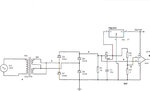
Bridge wave rectifier gives us full wave positive picks of 12V only.Diode D5 keeps capacitor charged. Op amp's inverting terminal takes reference before capacitor and it's non-inverting terminal takes reference after capacitor. So when Signal goes to zero, op amp's inverting terminal goes to zero. But op amp's non-inverting terminal takes reference after capacitor so it will goes to +12V. This situation is same as when you ground inverting terminal of op amp and feed some positive voltage to it's non inverting terminal, it will reflect +Vsat on output. So, you will get one spike of +12V in output when signal touch
We need the capacitor to feed constant voltage to voltage regulator so it must be high valued. You also need to see its voltage rating, its voltage rating also higher than 25V for better performance. I am also baffled about resistor selection.
D5 and C1 simply provide a DC voltage for the 12V regulator. R2 and R3 are the only critical parts. They set a threshold for defining "zero". It is not actually zero but about 2% of the peak of the fully rectified signal "B" (Vp in my diagram). The image shows how I come up with 2%. I assume the voltage on C1 is well filtered and equal to the peak of the rectified AC. Also, I ignore the drop across D5 but this could be subtracted from Vp for more accuracy. The idea of selecting R2 and R3 is to be just above zero. BTW, I am not sure R1 is necessary. The absolute values of R2 and R3 need to be big enough for low power dissipation but not too big to get issues with U2 bias current. Probably a good idea to add a large resistor from the U2 output to the U2 + input for hysteresis.
BTW, I agree with smijesh that the "dot" ends of the secondary windings need to be connected together. There is an error in this schematic.
This site uses cookies to help personalise content, tailor your experience and to keep you logged in if you register.
By continuing to use this site, you are consenting to our use of cookies.