Continue to Site

Welcome to EDAboard.com

Welcome to our site! EDAboard.com is an international Electronics Discussion Forum focused on EDA software, circuits, schematics, books, theory, papers, asic, pld, 8051, DSP, Network, RF, Analog Design, PCB, Service Manuals... and a whole lot more! To participate you need to register. Registration is free. Click here to register now.

Zero bias Transimpedance amplifier?

Status
Not open for further replies.

umery2k75

Advanced Member level 1
Joined
Apr 19, 2006
Messages
434
Helped
41
Reputation
80
Reaction score
15
Trophy points
1,298
Location
Pakistan
Activity points
5,748
Hello everyone,
To understand transimpedance amplifiers in more detail. I reverse engineered an electronic card of a photodiode amplifier of a machine which was not working because machine was scrap and probably made in around 1992 and It had few cards in it and few cards were lost and fortunately the photodiode card was present, so I took out the card and drew the schematic.
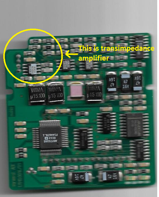
1676509237101.png


I removed all the components, so that I make no mistakes in drawing schematic. You can see.
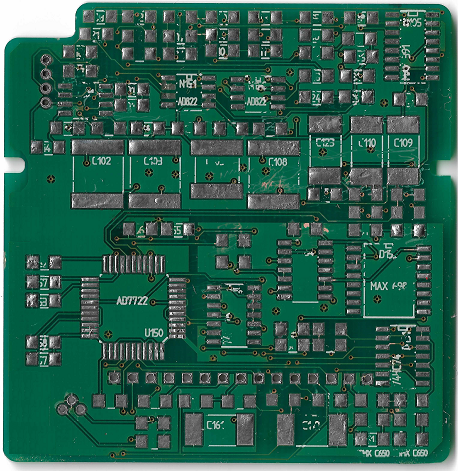
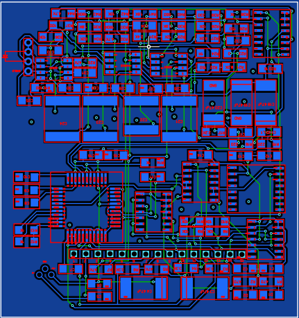
1676509527867.png


To this CAD version...

1676509604588.png


The reason I showed above pictures is to show my determination and whatever circuit I presents on EDABoard platform contains no error and no mistake. It is exactly the same schematic drawn from actual PCB.
The schematic of the circuit is like this. The lights falls on D1-D4 in forms of shadows and light, so the output must creates a modulating sine wave output. The higher the amplitidue of the sine wave - the higher the amplitude modulation.
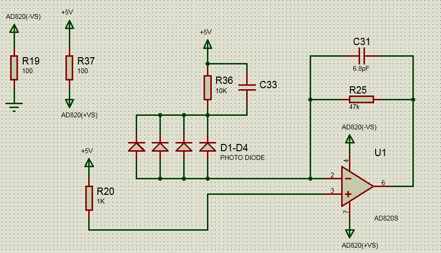
1676509893180.png


Note:
  1. I didn't measure the value of C31 and C33. I will measure it later, because it was not necessary at that moment. First to understand the schematic was important.
  2. This transimpedance amplifier seems like a zero bias to me, because +5V is appeared to be present at both Anode and Cathodes of the photodiode. How? I think because applying +5V at non-inverting input(+) will create a virtual +5V at inverting input(-) terminal. My logic is that in opamps circuits we makes virtual ground at inverting input in negative feedback, when we tied non-inverting input at 0V to ground, so if i tie +5V at non-inverting terminal, it will create virtual +5V at non-inverting input.

I really appreciate, if you could answer my following questions:

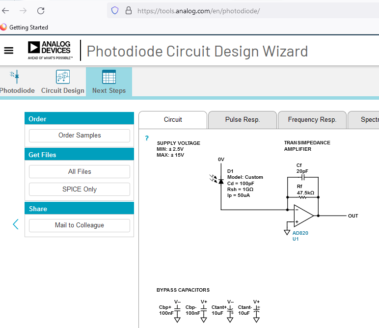
  • Why not connect photodiode cathodes to the 0V and similarly tie non-inverting input at 0V. As I used Analog Devices Photodiode amplifier wizard - it created a zero bias circuit for me, as you can see in the diagram below. This wizard is using the same opamp AD820.

1676510747049.png

  • Why power supplies of opamp are connected with 100ohms series resistors? +5V is connected through 100Ohms resistor, similarly ground is connected through 100Ohms resistor?
Thanks you so much for your time reading and understanding. I really appreciate your on coming advises and feedback.
 
Last edited:

The 100 Ohm resistors and there would be capacitors from -VS and +VS to ground are to filter noise from the supply rails. the current drawn by the IC would be very small so there would be negligible DC voltage drop across them.

The biasing looks suspicious, are you sure R20 connects to +5V and not 0V or there isn't another resistor from pin 3 to ground?

Brian.
The 100 Ohm resistors are connected to capacitors to create a low-pass filter. However, the opposite ends of these capacitors are connected to a 2.5V voltage reference instead of ground, and it's uncertain whether this still constitutes a valid low-pass filter configuration. The voltage reference is created using two 47uF capacitors, C18 and C19, and is connected to the cable shield of the photodiodes, resulting in the shield being pulled up to +2.5V. Although the shielded cable is only 6 inches long, the manufacturer drilled the stepper motor shaft to pass the sensor cable through the center of the solid shaft where the sensor cable enters at the tip of the shaft, travels through like a tunnel, and exits from the other end of the motor - a unique design. All electronics are mounted inside a heavy metal body with an IP67 rating, making it impervious to water damage and external noise. Therefore, there seems to be no clear reason to use the shielded cable for such a short distance, as there do not appear to be any other sources of noise that could affect the shield other than stepper motor itself.

1676794213003.png


This is the photodiode connector.
1676794419998.png


The biasing looks suspicious, are you sure R20 connects to +5V and not 0V or there isn't another resistor from pin 3 to ground?

I am 100% confident and sure. The biasing appears suspect to me as well. This is indeed the case, and the AD820 pin #3 is not connected to ground. Rather, it is connected to +5V through a 1K pull-up resistor, and there is no connection to ground in any way.

1676794945661.png


The second terminal of R20 goes to AD820 Pin#3.

1676795001025.png


I really appreciate your feedback on this.
 
Last edited:

Hi,

there are a lot of mistakes and wrong asumptions
(Refering to post#1)

Take pin3 of the AD820.
In the original design clearly shows a capacitor connected to pin 4.
--> Missing in your schematic.

Or top copper pour:
In the original design there are a lot of connected parts and vias.
--> missing all of them in your design.
This leads to a lot of unconnected parts in your design.
Like:
* resistor from pin4 (right pad)
* All three capacitors left of the 44 pin IC (left pads)
* and so on...

Klaus
and whatever circuit I presents on EDABoard platform contains no error and no mistake. It is exactly the same schematic drawn from actual PCB.
Just take the net on pin3 of the AD820 ... it seems to be a rather large net with at least ten parts connected. I just see one oart on your schematic.
This does not match at all.

Klaus
 

Hello KlausST,
I really appreciate all the help you've given me so far, and I'm sorry if my previous message came across as dismissive or critical. However, I still have some questions and concerns about the circuit, and I was wondering if we could discuss them further. The circuit block includes a transimpedance amplifier. Normally, a zero-volt bias is achieved by connecting 0V to the anode and the cathode to virtual ground, which is a common op-amp configuration. In this circuit, however, both the anode and cathodes are connected to +5V to achieve zero bias, which is my understanding of the circuit. The transimpedance amplifier output is a DC positive region modulating signal of sine wave. This signal is converted into straight square frequency by a separate op-amp, which can be read by the DSP controller to measure the frequency of the samples. The DSP controller is a key component in processing the signal data. The transimpedance amplifier is then fed into another amplifier stage to prepare the single-ended output for the gain and to be used with the AD7722, which accepts only differential input. To achieve this, other stages of op-amps are used to create a 180-degree out-of-phase signal of the amplified gain, converting the single-ended amplifier output to a differential-ended output, which can then be fed to a differential ADC that is both amplified output can be fed to the differential ADC in phase which is 0 degree and other is 180 out of phase. This ADC communicates with the DSP processor on the SPI bus. Additionally, there are pull-ups of 4.7K connected next to 180K ohm resistors after amplifier outputs and to other amplifier inputs. These are not connected with ordinary relays, but with solid-state analog switches. For the sake of schematic clarity, I drew the standard relay signals. Also, I believe this 4.7K pull-up may be connected because there are two modes of light operation in the machine - the first is the transmission mode, where the light passes through the sample and many IR LEDs are connected across the sample some 15 inches away, and the second is the reflection mode, where only 4 IR LEDs are connected to the sensor itself for when light cannot pass through the sample.

Take pin3 of the AD820.
In the original design clearly shows a capacitor connected to pin 4.
--> Missing in your schematic.
I hope below diagram clarifies.


1676875974715.png


In the original design there are a lot of connected parts and vias.
--> missing all of them in your design.
This leads to a lot of unconnected parts in your design.
Like:
* resistor from pin4 (right pad)
* All three capacitors left of the 44 pin IC (left pads)
* and so on...

The other parts of the circuits. I hope below diagram clarifies.
1676876058101.png


1676876709727.png


1676876659734.png

Really appreciate your feedback.
 

I hope below diagram clarifies.
It clarifies what I´m saying.
In the layout PIN3 is connected to C25, but not in your schematic.
In layout both (pin3 and right side of C25) is signal SHIELD, but not in your schematic.


The other parts of the circuits. I hope below diagram clarifies.
you ignored my headline:
Or top copper pour:
In the original design there are a lot of connected parts and vias. (to the copper pour!)
--> missing all of them in your design.

Klaus
 

It clarifies what I´m saying.
In the layout PIN3 is connected to C25, but not in your schematic.
In layout both (pin3 and right side of C25) is signal SHIELD, but not in your schematic.


you ignored my headline:
Or top copper pour:
In the original design there are a lot of connected parts and vias. (to the copper pour!)
--> missing all of them in your design.

Klaus


Thank you for your continued support. I want to clarify that I did not draw the schematic for the obsolete watchdog timer circuit, digital latch circuit, and clock circuit used to support the ADC. Instead, I focused on tracing the schematic for the amplifier section, which is the key part of the circuit. This is why you may find some things missing in the schematic.
Pin 3 is connected to a 1K resistor that pulls it up to +5V and is linked to the shield through a terminal for interference reduction, although it is not shown on the schematic. The unconnected vias on the PCB may serve for thermal reasons or other purposes. This is a two-layer PCB with no additional hidden layers.
The copper pour displayed on the PCB design software is not a true representation of the copper pour on the physical board, as there were only two copper pours on the board: one for digital ground and one for analog ground. During the schematic tracing process, I labeled "GROUND" next to the relevant component terminal to identify the ground connections and focus on tracing the schematic of amplifier section only
.
 

Status
Not open for further replies.

Similar threads

Part and Inventory Search

Welcome to EDABoard.com

Sponsor

Back
Top