Continue to Site

Welcome to EDAboard.com

Welcome to our site! EDAboard.com is an international Electronics Discussion Forum focused on EDA software, circuits, schematics, books, theory, papers, asic, pld, 8051, DSP, Network, RF, Analog Design, PCB, Service Manuals... and a whole lot more! To participate you need to register. Registration is free. Click here to register now.

Writing ADC data into DDR3RAM using Virtex7 fpga (vhdl)

Status
Not open for further replies.

rahdirs

Advanced Member level 1
Joined
May 22, 2013
Messages
424
Helped
93
Reputation
192
Reaction score
91
Trophy points
1,308
Location
Mordor
Activity points
4,492
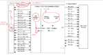
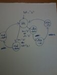
Problem: I have data sampled in an ADC at 337.5 MHz(actually it is sampled at 1335 MHz,but for sake of DDR3RAM i am slowing down the rate at which data comes out,using 1:2 demux provided within ADC) which needs to be written to a DDR3 RAM via a Virtex 7 fpga.(I am using Xilinx Vivado Design Suite)

My progress: To write data from Virtex 7 to DDR3 RAM, i used memory controller ip core given by vivado tool.After designing this,i need to give data from ADC to this memory controller module(some sort of interface).Can anyone help me with me with this ?
 

So my question is, 1) can i use traffic generator provided by Xilinx for my purpose or do i need to write a new traffic generator for my purpose ?
2) Even with traffic generator i would require a user interface or the example traffic generator itself is sufficient ?
 

The interface to the memory interface is the AXI protocol. So you need to write an AXI master that will send your ADC data to the memory controller. You may need an AXI Interconnect to share the memory controller with the Microblaze.

You can also open an example design that use the memory controller and start from there to build your architecture.
 

hi i am shrutireddy doing my mtech project . my project is same as yours can u help me with the vhdl code to write adc data to ddr3 ram through virtex 7 fpga ..pls .
if so pls reply to shrutireddyece@gmail.com
 

The interface to the memory interface is the AXI protocol. So you need to write an AXI master that will send your ADC data to the memory controller. You may need an AXI Interconnect to share the memory controller with the Microblaze.
I would have used AXI protocol to interface ADC with FPGA for transfering data at system level,but only for simulation in XIlinx vivado i'm instead thinking of using traffic generators.
 

What is your intention using this component? Testing your memory interface or your ADC component?

If it is to test your memory interface, it could work but I will rather go with an example design provided by Xilinx and modify the memory controller settings to fit my design. With the Microblaze, it will be easier to test the memory interface with the memory test example program.

If you want to test your ADC component. The traffic generator is no use. You may use instead the AXI Protocol Checker.
 

What is your intention using this component? Testing your memory interface or your ADC component?
I have data sampled in an ADC.I want to write that data into DDR3RAM using Virtex-7 fpga.(Why ?) use fpga is it is an existing architecture and there is no direct interface between adc & ddr3ram & i can't change design at this stage.

Ok,now this is how i understood the problem.Refer figure1 which shows 7 Series FPGAs Memory Interface Solution from Xilinx User Guide.I've added some names on interface. Are they correct ? And can i have my user interface in figure1(which i wrote as figure2) implement the state diagram of figure 2 ?
 

Attachments

  • Figure1.PNG
    Figure1.PNG
    34.3 KB · Views: 71
  • Figure2.jpg
    Figure2.jpg
    505.6 KB · Views: 68

From the figure 1, the user interface is used to connect to the memory controller. This interface can be configured to use the AXI4 protocol or you can keep this one as well. I would recommend to use the AXI4 interface.

If you want to implement the state diagram in figure 2, it must go in User FPGA Logic section. Basically, all you have to do is to gather samples from the ADC and pack them to match the interface data width. After that, you need to do a AXI4 write transaction to the memory controller. For more info in AXI4, refer to the AXI Reference Guide from Xilinx.
 

Hi,

On studying Xilinx ref manuals,this is what i understood:

There are three different interfaces that are supported by the generated memory controller.These are the Advanced eXtensible Interface 4 (AXI4) Slave Interface, the User Interface(UI) and the native interface.

As of now the AXI4 slave interface for the MIG is available only in Verilog,and not VHSIC HDL (VHDL) and i'm designing in vhdl.So,i'm going with UI.

In UI,how can we change ui signals like app_addr,app_wdf_data.By default app_wdf_data gets address as its data.How to change these ?
I tried changing DATA_PATTERN & CMD_PATTERN but this has no effect on app_* signals.
 

Both user interface (UI and AXI4) can be generated using VHDL. Currently, the memory controller core is generated in verilog but the wrapper of the core can be in VHDL. Make sure the vivado project language setting is in VHDL.

Note that to have acces to the AXI4 interface, the core should be included in a block design. Otherwise, only the "native" user interface is accessible from the ip catalog.

Try generate both options and looks for the provided example design. You should find useful information on how to use the core. Also, I don't see why you want to change the ui signal. You don't have to modify the core.
 

Both user interface (UI and AXI4) can be generated using VHDL. Currently, the memory controller core is generated in verilog but the wrapper of the core can be in VHDL. Make sure the vivado project language setting is in VHDL.

Even if i set my language as VHDL,as of now Vivado still generates AXI4 files in verilog.But i suppose you can always write the top wrapper file in VHDL.

Also, I don't see why you want to change the ui signal. You don't have to modify the core.

I don't want to change the ui signal.I just want to give it different values(user generated).
I have generated a list of sample ADC values in MATLAB.UI has some signals like app_wdf_data etc....I want to input these values into UI signal which will pass it onto MIG.

P.S:I've already written an ADC module which accepts the values from a text file into xilinx.
 

Status
Not open for further replies.

Similar threads

Part and Inventory Search

Welcome to EDABoard.com

Sponsor

Back
Top