Continue to Site
Follow along with the video below to see how to install our site as a web app on your home screen.
Note: This feature may not be available in some browsers.
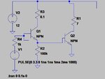
It's deadly necessary. And R3 must be increased to limit the Q1 current to the maximum permitted Q2 base current respectively 100 mA maximum BC109 current. Otherwise both transistors might be burned.What is R3 for?
Q2 takes 12/7 ~ 1.5A (1500 mA), so if its Hfe is 50, then it needs 30mA base current at .8V. If Q1 is to deliver 30 mA, then it needs 30/100(Hfe) mA ~ .3 mA at 1.6 V (two Vbes in series). Your processor can deliver 3.3 V, so at .3 mA, you have to drop 3.3 - 1.6 @ .3 mA = 1.7/.3 ~ 6K. You use 1K so it should work. Perhaps your working Hfes are too low.
What is R3 for?
Frank
It's deadly necessary. And R3 must be increased to limit the Q1 current to the maximum permitted Q2 base current respectively 100 mA maximum BC109 current. Otherwise both transistors might be burned.
Why don't you connect both transistors in REAL Darlington configuration?
Tie both collectors together.
Your circuit has to be designed to keep the maximum transistor ratings. The original circuit doesn't.But if R3 is increased, the current through Q2 decreases. And the voltage falling across becomes very low, so cannot increase R1.
Are you talking about the simulation or a real circuit? If it's the latter case, what's the Q2 transistor type?Its still not working anyway.
Your circuit has to be designed to keep the maximum transistor ratings. The original circuit doesn't.
Are you talking about the simulation or a real circuit? If it's the latter case, what's the Q2 transistor type?
BC109 has maximum continuous collector current of 100 mA, in contrast to 1.5 A required in your circuit. So it can't work and will be mosr likely destroyed if you try to switch the load.

BC547 has 300 mA maximum collector current rating, still not right.
LTSpice is about to foolproof by showing current and voltage ratings in the "pick-up transistor" selection. Don't ignore it.
I am using ZTX649 which has current capacity of around 2 A. Not using BC547. Please ignore BC547 in the image.
Which other differences between your real circuit and the LTSpice schematic should we expect?