tony_lth
Advanced Member level 5
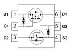
The picture is a Wall charging over-voltage protection component:
This is a typical component in mobile phone.
I have some questions for that:
(1). Why use NMOS? Just because the package of NMOS is smaller than PMOS?
(2). Why use two NMOS?
Thanks for the comments.
- - - Updated - - -
S1 is directly linked to S2.
G1 is directly linked to G2, and both are controlled by external signal.
D1 is current input, and D2 is output.