Continue to Site

Welcome to EDAboard.com

Welcome to our site! EDAboard.com is an international Electronics Discussion Forum focused on EDA software, circuits, schematics, books, theory, papers, asic, pld, 8051, DSP, Network, RF, Analog Design, PCB, Service Manuals... and a whole lot more! To participate you need to register. Registration is free. Click here to register now.

Why there have too big current?

Status
Not open for further replies.

wjxcom

Full Member level 5
Joined
Sep 7, 2005
Messages
281
Helped
4
Reputation
8
Reaction score
3
Trophy points
1,298
Activity points
3,840
Hi all, I'm designing a circuit as shown in figure 1:
Q196 is NPN transistor, the other transistors are PNP. The power voltage is 5V and 0V, the Base and Collector of Q343 is shorted together named netC who is connected to -5V.
When I simulate this circuit by SPECTRE, the current of Q321 and Q343 is about 85mA, but after tapeout, I test the chip, the the current of Q321 and Q343 is about 1A!! the current is so big.
Where does the big current come from? May be the circuit as shown in figure 1 is not correct? or something is wrong with Q321 and Q343? Q321 and Q343 have the same structor, the Cross-section of them is showned in figure 2,
E is emitter bipolar,
B is base bipolar,
C is collector bipolar,
Co_sub of Q 343 is connected to N1 as shown in figure 3
Co_sub of Q 321 is connected to N2 as shown in figure 3
In figure 3, Q1~Q4 are LPNP!
At the same time, the emitter area of Q343 and Q321 is big, the value is 12u*96u*3

Q495.PNG

Help me please, how can I decrease the current of Q343 and Q321? thanx!!

- - - Updated - - -

Because there have a negtive feedback loop (i.e. Q391,R55,Q196 and Q313), I don't think that the voltage value of net "netA" can be decreased, so the big current is NOT caused by "netA". In fact, "netA" is stable while I test the chip by the oscilloscope!
 

Some thoughts and questions:

netC=-5V is a pad, i.e. an external voltage (I hope)

  • May be the models don't reflect the reality correctly
  • How much is Co_sub voltage?
  • BP is a relatively low ohmic implant (at least with a higher concentration than BND), so all collectors are short-circuited?
  • Q343 is used as a diode in forward, so it tries to draw its emitter netB to (netC=-5V + 0.7V = -4.3V) , which isn't possible because of Q343's substrate voltage N1 (which probably is ≈ +1 .. 2V)
  • Q2 & Q4 are in reverse; is their BE (reverse) breakdown voltage modeled correctly?
 
  • Like
Reactions: wjxcom

    wjxcom

    Points: 2
    Helpful Answer Positive Rating
If the current gets big early (like less than 2V) I'd look to
some problem with the numerous isolation junctions, maybe
the biasing has one or more of them forward instead of
reverse. If it gets big abruptly and over 3-4V I'd ask about
the transistor BVceo/BVcbo which on some advanced nodes
has gotten to below 5V (narrow base punchthrough) even
though the individual diodes (BVebo, BVcbo) may be higher.

Pulling some curves for relation of current to the supplies
(and I'd do them independently in the interests of chasing
down the specigic actor(s)) ought to be enlightening.
 
  • Like
Reactions: wjxcom

    wjxcom

    Points: 2
    Helpful Answer Positive Rating
Hi erikl,
1.yes, netC is a pad
2.Yes, all collectors are short-circuited.
3.I think Q2 & Q4 BE (reverse) breakdown voltage modeled correctly, because if netC is 18V, the chip has NO current!!
3.Co_sub is connected to net N1(see figure 3), from SPECTRE simulation, the voltage of Co_sub is 4.7V. But while I test the chip, if netC is -5V, Q2 and Q4 have big current too!! we can see the resule below:
bigcurrent.PNG

- - - Updated - - -

Hi dick_freebird: I'm sorry my English study is shabby!, May I ask you that what's the meaning of "If the current gets big early (like less than 2V)"? I do not know who is "like less than 2V"! help me ple, thanx!!:oops:
 
Last edited:

Hi erikl:Q343's substrate voltage is 0, i.e. GROUND, rather than N1, but Q343's Co_sub voltage is N1!
 

Hi dick_freebird, I test the chip again, the current is big abruptly and over 3.2A. So I think there have punchthrough. But which transistor is punchthrough? Q343 or Q321?
 

... the current is big abruptly and over 3.2A. So I think there have punchthrough. But which transistor is punchthrough? Q343 or Q321?

Try and let Spectre tell their different node currents.

Pls. check your complemented circuit:
wjxcoms_circuit_modified.png
 
  • Like
Reactions: wjxcom

    wjxcom

    Points: 2
    Helpful Answer Positive Rating
Hi erikl: thanx for your post, but why Q343 have a net connects to 0V?
 

... why Q343 have a net connects to 0V?

Do you measure this big current between GND (0V) and netC=-5V ?

I guess your cross-section image shows one single PNP transistor, i.e. a triple transistor with common collector, common base & common emitter contacts (e.g. Q343), and you use several such transistors, right?
 
  • Like
Reactions: wjxcom

    wjxcom

    Points: 2
    Helpful Answer Positive Rating
Hi erikl: the current between GND and netC is a little bit smaller than the current between GND and VDD(5V)

In fact, the cross-section image of Q343 shows three PNP transistor, i.e. there have three PNP transistor, whose collector, base & emitter contacts together.
 

Hi wjxcom, pls. s. below:

Hi erikl: the current between GND and netC is a little bit smaller than the current between GND and VDD(5V)
Which means, the main current goes directly from +5V to -5V , apart from a small part which goes directly from +5V to GND, the latter one through Q313 , several current sources and resistors. Hence the main current goes through the transistors Q1 .. Q4 , and Q321 & Q343 . Check all these currents uniquely!

In fact, the cross-section image of Q343 shows three PNP transistor, i.e. there have three PNP transistor, whose collector, base & emitter contacts together.
Yes, I thought so. Don't be irritated by my two Co_sub connections in your image: I know they go to different BND isolation implants of different transistors.
 
  • Like
Reactions: wjxcom

    wjxcom

    Points: 2
    Helpful Answer Positive Rating
Hi erikl: In fact, the most current goes through the transistors Q1~Q4 ,Q321 & Q343, as shown by the picutre which I uploaded in #4. In that picture, the color of this transistors is red which meas the current is very big!
 

Sure: As Q2 & Q4 are in reverse and work as (collector-assisted) e-b reverse breakdown Z-diodes (s. my post #2), and Q1 & Q3 are in full saturation (Vce=0.3V), and there is no actual current limitation in these branches, a rather high current is to be expected, only limited by internal bulk resistances.

And probably netA is low enough to open Q321 sufficiently to sustain a similar high uncontrolled current through it and Q343 which works as a collector assisted diode.

Did you try and analyze the circuit by simulation?
 
  • Like
Reactions: wjxcom

    wjxcom

    Points: 2
    Helpful Answer Positive Rating
Hi erikl: yes, I do analyze the circuit by simulation, and I don't think the simulation is useful. From simulation, Q1~Q4 have no current, the current of Q321 and Q343 is only 80mA. But from testing result, the current is so big!! and from the testing result I think there have big current from Co_sub to the collector of Q343 (but the current should never existed!! because the Co_sub and collector of Q343 is a reverse diode).
 

Hi wjxcom,

I do analyze the circuit by simulation, and I don't think the simulation is useful. From simulation, Q1~Q4 have no current, the current of Q321 and Q343 is only 80mA. But from testing result, the current is so big!!

Probably the transistors aren't modeled correctly, especially their collector-to-Co_sub parasitic diodes, pls. s. below.

... from the testing result I think there have big current from Co_sub to the collector of Q343 (but the current should never existed!! because the Co_sub and collector of Q343 is a reverse diode).

Both the collector BP and the Co_sub BND implants probably are rather highly doped, BND impurity concentration might be > 1017 cm-3, hence their reverse breakdown voltage (by tunneling mechanism) might be around 5V or even lower, s. the figure below (Si abrupt junction breakdown voltage at 5*1017 cm-3 is 5V). Probably this isn't modeled correctly, but it might generate such high breakdown current.

View attachment breakdown voltage vs. impurity concentration__from_Sze-Physics_of_Semiconductor_Devices_6th_edit.pdf
 

Hi all, Hi erikl:I'm glad to see you again!
It's cost me so long time to analyse the big current, now I want to write something:
At first, upload two figure again:
???1.png???.png

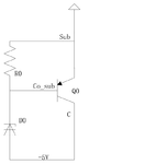
Look at these two figure: the left figure is a bipolar Q1, but in this bipolar, there have a parasitic transistor Q0 whose emitter is Sub, base is Co_sub and collector C. Notice: C is the collector of bipolar Q1 too! the parasitic transistor Q0 was shown in the right figure. In the right figure, there have a parasitic resistor R0 between Sub and Co_sub, and a reverse saturation current Is between Co_sub and C (Is was molded by a diode)!

When C is connected -5V, Is i.e. the reverse saturation current flowing through the parasitic resistor R0. If Is is big, the Vbe of Q1 is big, Q1 is turned on and a big current passes through Q1.

But I don't know if my ideal is right or not, so help me please, thanx!!

- - - Updated - - -

Again: How can I get rid of the reverse saturation current Is by layout?
 

Hi again wjxcom!

I don't know if my ideal is right or not, so help me please, thanx!!

I think your parasitic transistor Q0 is nothing else as your (intended) transistor Q2 (or Q4), which are connected in reverse between E and C. As you know such a transistor acts in reverted connection (E and C exchanged, still PNP) like such a transistor with a low amplification factor.

So it depends on the reverse current capability of the B-C (related to Q0) or Co_sub to Psub reverse junction current and the value of the (parasitic) resistance R0 between the B-E connection, and the (reverse) current amplification factor of Q0 .


- - - Updated - - -

Again: How can I get rid of the reverse saturation current Is by layout?
Try if there is a meaningful current rise when you slowly increase the voltage between Co_sub and Sub - if you have access to Co_sub. If so, this would mean a rather low reverse breakdown voltage between the BND and Psub junction (which is not usual).

You could perhaps try and reduce the R0 resistance by more connections between their nodes in the layout.

Can you reduce the overall size of the Q2 & Q4 transistors?
 

Hi erikl: from the foundry process datasheet, the size of Q2 &Q4 can not be reduced any more. Maybe the only thing I can do is more connections between Co_sub and metel one in the layout to reduce R0.

For the transistor Q321, I can't access Co_sub, but I can disconncet all connections of Co_sub, at the same time, I can slowly increase the voltage of the Collector from 0V to -5V, there is a meaningful current rise, I think this phenomenon can also means a rather low reverse breakdown voltage between the BND and Psub junction.

Finally, do you mean that my ideal is not correct enough and there have no parasitic bipolor Q0? thanx!!!
 

from the foundry process datasheet, the size of Q2 &Q4 can not be reduced any more.
Then I'd think Q2 & Q4 are nothing else than the BP-BND-Psub parasitic PNP transistors below their upper PNPs. And they should anyway be depicted like your Q0 (collector Psub has the lowest doping concentration, emitter BP the highest).

Maybe the only thing I can do is more connections between Co_sub and metel one in the layout to reduce R0.
Right; but don't connect to Sub, as shown in the Q0 figure (= Psub , according to your first figure above), because this is the most negative voltage. I think you should connect it to the collectors of Q1 (net N1) respectively of Q3 (net N2). And right: as many metal connections as possible.

For the transistor Q321, I can't access Co_sub, but I can disconncet all connections of Co_sub, at the same time, I can slowly increase the voltage of the Collector from 0V to -5V, there is a meaningful current rise, I think this phenomenon can also means a rather low reverse breakdown voltage between the BND and Psub junction.
In this part of your circuit I think the reason for the meaningful current rise is just the non-negligible current gain of Q343.

Finally, do you mean that my ideal is not correct enough and there have no parasitic bipolor Q0? thanx!!!
Of course there are unavoidable parasitic PNP transistors like Q2 & Q4 (which I think should be replaced by a reversed circuit like Q0) each as large as the overlying triple PNPs. You need to characterize them as PNPs with relatively low current gain, and you know their area. Would be good, if you could get hold of doping concentrations and thicknesses of their layers.
 

Status
Not open for further replies.

Part and Inventory Search

Welcome to EDABoard.com

Sponsor

Back
Top