Continue to Site

Welcome to EDAboard.com

Welcome to our site! EDAboard.com is an international Electronics Discussion Forum focused on EDA software, circuits, schematics, books, theory, papers, asic, pld, 8051, DSP, Network, RF, Analog Design, PCB, Service Manuals... and a whole lot more! To participate you need to register. Registration is free. Click here to register now.

Why the voltage @ gate is +11V

Status
Not open for further replies.

siddharthtaunk

Junior Member level 1
Joined
Apr 10, 2013
Messages
18
Helped
0
Reputation
0
Reaction score
0
Trophy points
1,281
Activity points
1,432
Hello,

Kindly help.

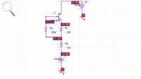
I have attached a circuit.

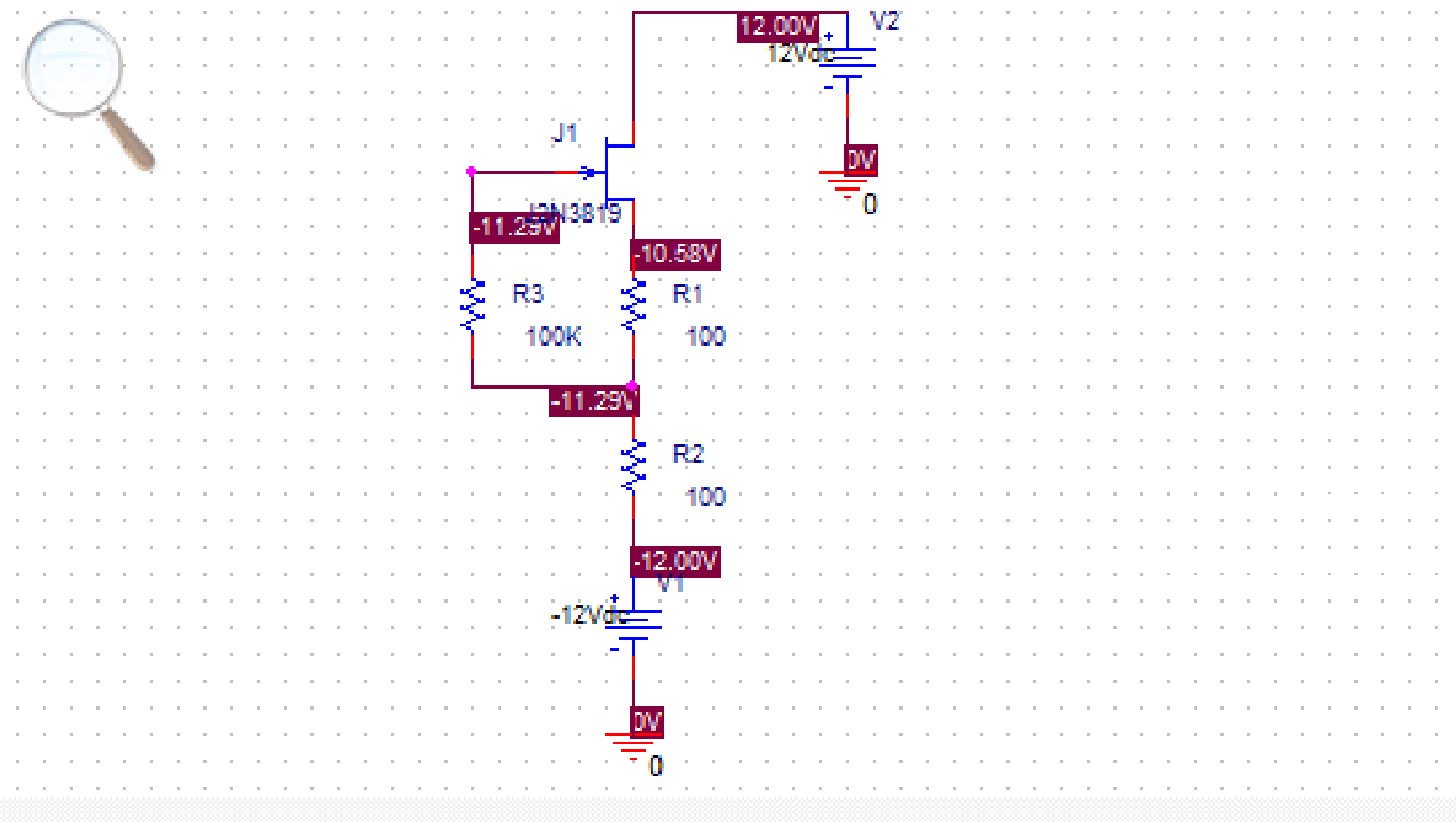
Please see that the gate voltage is -11V(approx).

Why is that so. I have an 100K resistor between the Gate and the point of resistor divider.

What i assume is NOTHING at the GATE pin (0V)

I have seen the same result in orcad and was perplexed.

Please help me out. Its urgent.

Thank you all in advance.

Siddharth


There is not 0V on the gate, as the gate has no reference to GND.
The only connection to gate is essentially -12V (assuming ideal FET). Hence the ~-12V on the gate :)

You need to add a reference to GND (e.g. through a resistor) or a dignal path to +12v to change the gate voltage.
In case you do actually need 0V (GND) on the gate, replace gate-source resistance with resistor to GND.

/DLakji.
 

Re: Why the voltage @ gate is -11V

..._thumb.jpg pictures are thought of as icons and practically are illegible. Please link to the original!
 

Hi,

you have two voltage sources.
One at the top, the other at the bottom of the picture.

The voltage at the bottom voltage source is set to "-12V". Set it to "+12V"

Klaus
 

Hi,

you have two voltage sources.
One at the top, the other at the bottom of the picture.

The voltage at the bottom voltage source is set to "-12V". Set it to "+12V"

Klaus

Klaus thank you very much for your reply.

The negetive supply is for biasing the fet.

But can you please explain me the solution a bit more for a better understanding.

Thanks

Siddharth
 

Hi,

(If i need negative voltage i`d turn the battery sign upside down and set voltage to 12.0V...but the function is the same..)

Let´s go step by step.

it is a depletion mode FET and it is slightely conductive, so there is a I-DS of about 7.1mA

Now from the bottom:
* There is the GND symbol. This is the voltage reference. It is 0V fixed.
* Then there is a battery. The "+" sign at the top, but with the voltage setut to "-12V" you get a "-12V" reading at the top.
* then 100R. Gate current through R3 is 0.0A. Current through FET is about 7.1mA. Causing a voltage drop of 0.71V: -12V-(-0.71V) = -11.29V
* then R3 to gate. No current, no voltage drop: therfore the same -11.29V
* then R1: again 7.1mA giving a voltage drop of 0.71V: -11.29V - (-0.71V) = -10.58V
* FET: Voltage at Gate: -11.29V, Voltage at Source: -10.58V giving a V_GS of -0.71V

What else do you want to know?

Klaus
 

Thank you very very much Klaus.

and Thanks to EDABoard
 

I have one more question

When i ground the gate (0 volts) of the fet, heavy current flows through the device. More than 40ma
40ma. Otherwise it is mere 4ma

What is the solution????
Thanks in advance

Siddharth
 

Status
Not open for further replies.

Part and Inventory Search

Welcome to EDABoard.com

Sponsor

Back
Top