Continue to Site

Welcome to EDAboard.com

Welcome to our site! EDAboard.com is an international Electronics Discussion Forum focused on EDA software, circuits, schematics, books, theory, papers, asic, pld, 8051, DSP, Network, RF, Analog Design, PCB, Service Manuals... and a whole lot more! To participate you need to register. Registration is free. Click here to register now.

Why the tail resistor can increase the amp's stability

Status
Not open for further replies.

fanrong

Banned
Joined
Oct 20, 2006
Messages
122
Helped
3
Reputation
6
Reaction score
1
Trophy points
1,298
Activity points
0
Hi,everyone :
I read a patent (US6407537) , it is said that the tail resistor can increase
the stability . May anyone explain it ?
26_1170235850.GIF
 

My educated guess would be:

Increasing RTL will decrease the transconductance of the input pair and the UGF will go down which will increase your phase margin.
 

Yes, i agree.

But what's the subject of the patent ? The current-splitting mirror in the second stage ? It works as a current multiplier?
 

What's the purpose of T7 and T8 ? They work as current source !
 

provides a feedback path, whats your level of engineering understanding, i'm not sure how technical i can get in explaining this, are you familiar with root locus or nyquist plots?
 

T7 and T8 are supposed to work as a current source,to bias the input pair without losing input commond mode range due to voltage drop in Rtl.

I am curious about T13 T14 T11 T12.

In pair t13 and T14 one can do a 1:N mirror, and then have N times more current
in T11, where again one can do 1:K mirror and get N*K times more current,
but I don't see the reasoning there. One can have a different supply (higher voltage?) for the pair T11-T12, but I see a much reduced headroom for T13.

Anyone can say more about this ?
 

Hi , n1cm0c :

Why you said "T7 and T8 are supposed to work as a current source,to bias the input pair without losing input commond mode range due to voltage drop "
Can you explain it more ?

And what is the gain of the amp (T1,T2,T3,T4,T6,T7,T8)?
I still can 't understand why the RTL increase the stability .
 

Can anyone tell what is the gain of the amp composed of T1,T2,T3,T4,T6 ?
 

I think the feedback of the OA is positive, isn't it?
 

renwl said:
the feedback of the OA is negative. there is no problem.
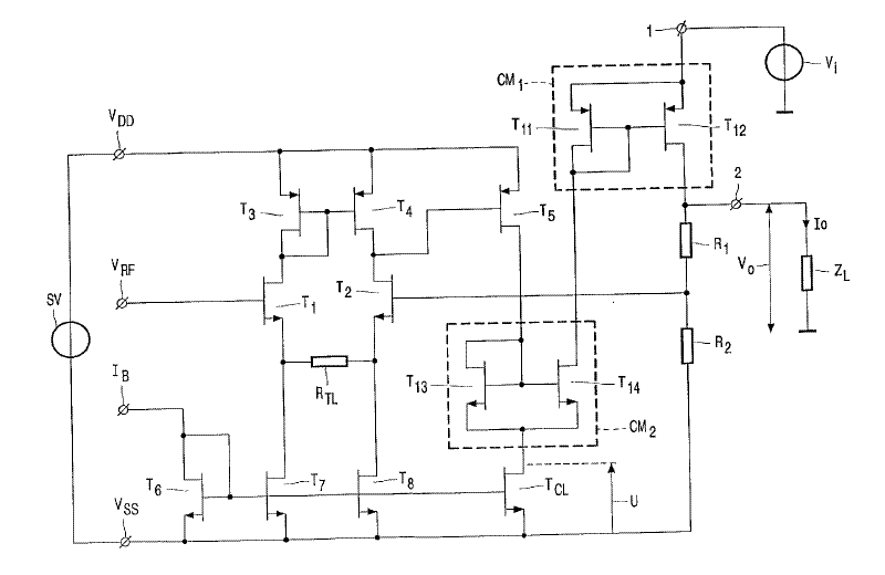
My analysis is as below.
I suppose VT2_G( voltage of the gate of T2) decrease, and VT8_D decrease, and the current from left to right flow through RTL will increase, and IT2D decrease, and IT3D increase, and IT4D increase, so VT5_G increase, IT5D decrease,IT13D and IT14D decrease, IT11D decrease, IT12D decrease. Finally, VT2_G decrease.
So it's positive feedback. If something is wrong in my analysis, please tell me, thanks.
 

less IT5D means that IT13D decrease and IT14D increase.
so the voltage of the gate of T2 will increase.
it's negative feedback.
 

The added R is called source degenarated resistor, it will reduce the gain of differential pair, and increase it's input range. Reduce gain will increase stability too.
But the circuit is still 2 pole system, some kind of compenstaion is needed except u make the gain of first stage very low (i.e. the non-domainant pole far away ur dominant pole).
 

I think IT13D should equal to IT14D, because they share the same gate and drain, and they are all in saturation region.
 

But if there is no RTL , the gain will be more samller for the high output R
of current source . So I think the RTL will increase the stability by decreasing
the gain is wrong !
 

Had u run the simulation of that amp ?
What's the phase margin & DC gain ?
I don't understand why the gain will be larger without RTL?
Can u show us ur simulation of derivation ?
 

If there is no the RTL , the transconductance will be :
Gm = gm /1 + gmro
where gm is the transconductance of the input device, ro is the output
resistor of the current source .
For ro is very big , t
Gm = 1/ro
But if there is RTL ,
then
Gm = gm/[1 + gm(RTL/2] = 2/RTL
So if there is no the RTL , the gain should be small .
 

fanrong said:
If there is no the RTL , the transconductance will be :
Gm = gm /1 + gmro
where gm is the transconductance of the input device, ro is the output
resistor of the current source .
For ro is very big , t
Gm = 1/ro
But if there is RTL ,
then
Gm = gm/[1 + gm(RTL/2] = 2/RTL
So if there is no the RTL , the gain should be small .

Why the Gm of differential pair without RTL is 1/ro ?
if it was true , then u will always get output gain as Gm*ro=1 ?
The Gm should be equal to gm , such that without RLT ur first stage should
have gain gm*ro !
 

without RTl means you should replace this resistor with a short line.
and it is a virtual ground at this point for diffrecial circuit

then you should recalculate you Gm:D

fanrong said:
If there is no the RTL , the transconductance will be :
Gm = gm /1 + gmro
where gm is the transconductance of the input device, ro is the output
resistor of the current source .
For ro is very big , t
Gm = 1/ro
But if there is RTL ,
then
Gm = gm/[1 + gm(RTL/2] = 2/RTL
So if there is no the RTL , the gain should be small .
 

T1 T2 T3 T4 are standard differential input with current mirror load.

if RTL is zero, then T7 and T8 are two current sinks in parallel. If RTL is non-zero then it's also a standard configuration, and the fact that the bias currents do not go through it keep the input common mode range unchanged.

T5 is a standard second-stage, common source. The load of T5 is not directly
TCL, which would be the standard, but T13 and T14. The way they are connected
the input resistance looking from the drain of T5 into T13 is 1/gm + (N+1)*Ro,
where Ro is the output resistance of TCL. The N is the multiplication factor of the mirror. There's no net increase by doing this, since the current in TCL is increased also by (N+1) , so its Ro was divided by (N+1). Adding T13 and T14 has then another function.

In small signal, it copies current variations in T5 to T11, and T11 copies it to the output with T12. One could then multiply currents by N and then by K in these two mirrors, and use a different supply (higher voltage?) at the output.

The problem is, as already pointed out, that the feedback back to T2 seems to be positive. If T12 sources current into the resistive divider the voltage there will rise, but if if does not then the node will fall to some voltage between the external ground (where ZL is) and VSS. consider TCL a short to ground , and notice that the drain of T5 rises and falls together with the output, to see that the connection
back to T2 makes the feedback positive.

What is the purpose of the circuit, in the patent?
 

Status
Not open for further replies.

Part and Inventory Search

Welcome to EDABoard.com

Sponsor

Back
Top