Continue to Site

Welcome to EDAboard.com

Welcome to our site! EDAboard.com is an international Electronics Discussion Forum focused on EDA software, circuits, schematics, books, theory, papers, asic, pld, 8051, DSP, Network, RF, Analog Design, PCB, Service Manuals... and a whole lot more! To participate you need to register. Registration is free. Click here to register now.

Why source resistance is too big in the common source amplifier?

Status
Not open for further replies.

anhnha

Full Member level 6
Full Member level 6
Joined
Mar 8, 2012
Messages
322
Helped
4
Reputation
8
Reaction score
4
Trophy points
1,298
Visit site
Activity points
3,684
Why source resistance is too big and poles problem?

Hi.

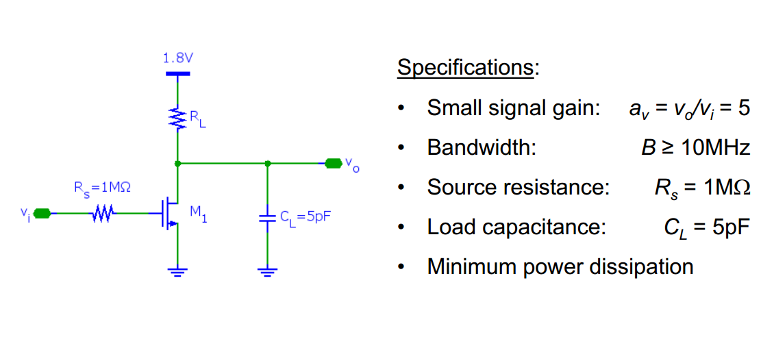
I am reading an example design using gm/id methodology. The below is a common source amplifier with given specifications.
What is confusing here is why the source resistance is too big up to 1MΩ. I think it should be several ohms!
Could you explain? Thanks.
9770901700_1404627251.png


- - - Updated - - -

Also, I have another problem with this circuit. Hope you could help. I attached the lecture for reference. Thanks.

attachment.php
 

Attachments

  • gmid common source.PNG
    gmid common source.PNG
    97.5 KB · Views: 598
  • 2011-12 OTA gm Id.pdf
    898.4 KB · Views: 124

The error in reasoning is to assume that the specific component values used in the example circuit have any general meaning.

I think, the example is discussing the special case where an amplifier is for some reason driven by a high impedance source and calculates the bandwitdh limitation caused by the source resistance. The schematic is misleading in so far as it doesn't show the resistance as part of the external source.

The calculation is also incorrect for all FETs with non-neglibible Cdg capacitance, where the bandwitdh is considerably influenced by the miller effect.
 
  • Like
Reactions: anhnha

    anhnha

    Points: 2
    Helpful Answer Positive Rating
Thank you.

If the input pole is the dominant pole, then shouldn't it be gm> 2*pi*B*Cgs?
 

Hi anhnha,

1.) Yes - your assumpton is correct. Your formulas (red square) do apply.
2.) Introducing the gain |Av|=gm*RL into the second unequality you get: gm>2*Pi*B*CL*Av.
3.) Regarding the large Rs value: There must be a special reason I do not know. Perhaps just an introductory exercise?
 
  • Like
Reactions: anhnha

    anhnha

    Points: 2
    Helpful Answer Positive Rating
Thank you very much!
I have a question relating to #2. Your formula is gm > 2*pi*B*CL*Av but the formula in the article is gm > 2*pi*B*CL. Why Av is equal to 1 here?
Are input and output poles conditions used to assure that these poles don't locate in the range of 0 to B (Hz)?
 

Well, thanks! I was confused because the author also use that expression for numerical calculation in the article.

- - - Updated - - -

Could you guide me sizing the mosfet using gm/id method?
 

Well, thanks! I was confused because the author also use that expression for numerical calculation in the article.
- - - Updated - - -
Could you guide me sizing the mosfet using gm/id method?

@1: Perhaps the author has not used the classical definition for the bandwidth B (gain -3 dB down) but the frequency where the gain is unity. In this case, his formulas are OK.
@2: Sorry, I can´t.
 

Hi anha
I think B is bandwith (3dB) not gain bandwith. The author want to put input and output poles stay away from 3dB pole to make sure good phase margin
 

A few random notes here:
- the source resistance is large to make the problem harder: you cannot tell if the dominant pole is at the input or at the output
- since you cannot tell which pole is dominant, you need to have constraints for both poles to be above the 3dB bandwidth (this has nothing to do with stability as you cannot make this circuit unstable)
- The observation about missing Miller cap and other hidden assumptions are pertinent but justifiable (the slides tell you that out of neglecting "self-loading" you'll have to increase ft)
- the av in the gm constraint seems really missing and that's hard to justify
- there are better ways to use gm/Id method by introducing inversion coefficients and technology currents; that way a lot of calibration plots will not be necessary
 

Status
Not open for further replies.

Part and Inventory Search

Welcome to EDABoard.com

Sponsor

Back
Top