cupoftea
Advanced Member level 5
Hi,
We have a PCB to bring up from a customer (their engineer left)
It’s a 300W Synchronous Pushpull, 24vin, 32vout, each Pri FET switches at 153kHz.
Transformer is planar and 1:2 (pri:sec)
The Pri FETs are SMD as follows…
https://www.infineon.com/dgdl/Infin...N.pdf?fileId=5546d4627617cd8301762e04616a61b8
The Sec Sync FETs are SMD as follows…
https://www.infineon.com/dgdl/Infin...N.pdf?fileId=5546d46277921c320177aa5221467dea
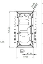
The PCB is enclosed in a thick walled aluminium enclosure on all 6 sides. Walls are some 1cm thick all round.
However, bizarrely, neither primary FETs, nor secondary Synch FETs, are actually directly heatsunk to this enclosure. Both Pri and sec side FETs are actually mounted on the underside of the PCB, and via “gouges” in the bottom aluminium, they get gap-padded via their top surface to the bottom of the alu enclosure. (the "gouges" being needed because the FETs obviously stick out from the bottom surface of the PCB)
As you know, the Gap pad forms a relatively poor thermal pathway from FET tops to alu base.
{Incidentally, the Planar transformer woudl also be gap-padded to the enclosure base...there is a cutout in the PCB for it.
It’s a 4 layer board and the pri fets have thermal vias to top copper, and these thermal vias traverse copper pours on all 4 planes.
The secondary FETs have no thermal vias, but there is copper planes on all 4 layers “above” it. On the top layer, directly above the secondary FETs, lies an SMD inductor dissipating 3W (IHLP8787)
Why have they not gone the “standard” route and had top mounted SMD FETs, with thermal vias to bottom copper, then 6um thick thermal/insulation pad to the thick metal enclosure base?
I am thinking the only reason would be fear of common mode emissions, but if that scares them, then why is there no input common mode choke?
So , Can you think of a reason for not making best use of the thick aluminium enclosure for heatsinking these 4 FETs?
We have a PCB to bring up from a customer (their engineer left)
It’s a 300W Synchronous Pushpull, 24vin, 32vout, each Pri FET switches at 153kHz.
Transformer is planar and 1:2 (pri:sec)
The Pri FETs are SMD as follows…
https://www.infineon.com/dgdl/Infin...N.pdf?fileId=5546d4627617cd8301762e04616a61b8
The Sec Sync FETs are SMD as follows…
https://www.infineon.com/dgdl/Infin...N.pdf?fileId=5546d46277921c320177aa5221467dea
The PCB is enclosed in a thick walled aluminium enclosure on all 6 sides. Walls are some 1cm thick all round.
However, bizarrely, neither primary FETs, nor secondary Synch FETs, are actually directly heatsunk to this enclosure. Both Pri and sec side FETs are actually mounted on the underside of the PCB, and via “gouges” in the bottom aluminium, they get gap-padded via their top surface to the bottom of the alu enclosure. (the "gouges" being needed because the FETs obviously stick out from the bottom surface of the PCB)
As you know, the Gap pad forms a relatively poor thermal pathway from FET tops to alu base.
{Incidentally, the Planar transformer woudl also be gap-padded to the enclosure base...there is a cutout in the PCB for it.
It’s a 4 layer board and the pri fets have thermal vias to top copper, and these thermal vias traverse copper pours on all 4 planes.
The secondary FETs have no thermal vias, but there is copper planes on all 4 layers “above” it. On the top layer, directly above the secondary FETs, lies an SMD inductor dissipating 3W (IHLP8787)
Why have they not gone the “standard” route and had top mounted SMD FETs, with thermal vias to bottom copper, then 6um thick thermal/insulation pad to the thick metal enclosure base?
I am thinking the only reason would be fear of common mode emissions, but if that scares them, then why is there no input common mode choke?
So , Can you think of a reason for not making best use of the thick aluminium enclosure for heatsinking these 4 FETs?