Continue to Site

Welcome to EDAboard.com

Welcome to our site! EDAboard.com is an international Electronics Discussion Forum focused on EDA software, circuits, schematics, books, theory, papers, asic, pld, 8051, DSP, Network, RF, Analog Design, PCB, Service Manuals... and a whole lot more! To participate you need to register. Registration is free. Click here to register now.

why my bandgap voltage looks like below?

Status
Not open for further replies.

lxcpku

Junior Member level 3
Joined
Sep 7, 2007
Messages
30
Helped
0
Reputation
0
Reaction score
0
Trophy points
1,286
Activity points
1,508
bandgap offset voltage

why my bandgap voltage looks like below?
i think it should be lke a parabola and will be change with different resistance values
i have checked all the transistors in the saturation region


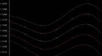
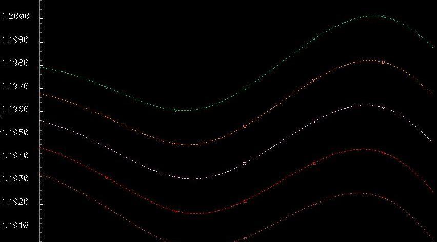
in the design above,the ratio of pnp transistor i used is 2:1
however, when i changed the ratio of pnp transistor from 2:1 to 8:1 and modify the resistance value accordingly, i got another pic which is a parabola . what surprised me is the voltage fluctuation with the temperature of the two design is equal, that is 3mv, but why ? anyone can help me ? thx in advance
 

2nd order bandgap design

you can upload your schematic.Maybe you have a curvature compensation.it's a wonderful result!
 

Generally, this results is good. But this results can be related with factors that can lead to bad behavioural during another kind of simulation. E.g. to be sure u should check how ur circuit sensitive to supply variation.

P.S. Ratio 2:1 too small I think. The lager ration can helps you to eliminate influence of error amplifie offset.
 

DenisMark said:
Generally, this results is good. But this results can be related with factors that can lead to bad behavioural during another kind of simulation. E.g. to be sure u should check how ur circuit sensitive to supply variation.

P.S. Ratio 2:1 too small I think. The lager ration can helps you to eliminate influence of error amplifie offset.


i have checked the influence of supply variation to my bandgap voltage. it is good since i used folded cascode in OTA.
just like u said,2:1 is too small,a larger ratio should be better. however ,i am puzzled by the different curve with differnet pnp ratio (of course , resistance value also modified to obtain the smallest variation against temperature)
 

Your result shows it have a good performance and it have 2nd order curvature compensation. Keep the design, it should not be a problem.


If you do not design for 2nd order compensation , I have two questions to ask:

Do you use the same type of resistor for all the resistors in the bandgap?

Do you add a resistor at the base of the bipolar transistor?
 

WindRay said:
Your result shows it have a good performance and it have 2nd order curvature compensation. Keep the design, it should not be a problem.


If you do not design for 2nd order compensation , I have two questions to ask:

Do you use the same type of resistor for all the resistors in the bandgap?

Do you add a resistor at the base of the bipolar transistor?

resistors i used in the bandgap are of the same kind, that is nwell resistor
and i did not add resistor at the base of the bipolar transistor
 

Have you read this post ?
What ratio of resistor do u have? What expected offset of amplifier? Is results after Monte-Carlo simulation acceptable for you?

Obtained result related with operation region of bipolar transistors. U can try to achieve same operation for another retio. May be it possible.
 

Hi, I can see you almost have 1.19 V & the variation is too small so < I can say it's accepted
best regards,
Rania
 

DenisMark said:
Have you read this post ?
What ratio of resistor do u have? What expected offset of amplifier? Is results after Monte-Carlo simulation acceptable for you?

Obtained result related with operation region of bipolar transistors. U can try to achieve same operation for another retio. May be it possible.

The post you suggested is very helpful. I havenot considered the effect of resistor's ratio to offset voltage. I just ran simulation in all corners and did not run Monte-Carlo simulation .
BTW:Is it necessary to run post simulation? i think i should,but many people say that is no necessary

thx a lot :)
 

One fast way to check the effect of the Bandgap opamp without running MC analysis is to insert a dc offset voltage at the input of the opamp. That will be able to see the effect of bandgap due to offset.

This is normally done if you donot have MC analysis in your EDA tools or the process does not support MC analysis as the process need to define amount of mismatch between devices.

Added after 18 minutes:

hi lxcpku

After thinking for so long on your temperature curve, I still does not understand how come if you design a first order bandgap, you can get a 2nd order bandgap. I guess it will be good if you can understand what is the reason and share with us.

In my years of design, I have see only 1 order bandgap behaves as 1st order (parabolic) except they have problem when the temperature is higher than 120degrees, the curve start to increase very fast. The reason I guess is at high temperature, the models may not be so well modelled. It is not the case in measurement.

Please share your finding if you have any.. Thanks.
 

Hi, lcxpku, your BGR really looks so strange, I havn't ever seen this kind of bang-gap curve. Most of the curves raise from -40~40, and falls from 40~100, 2nd-order BGR would raise a little from 120~150.
I have ever designed a BGR with a 1st structure, in simulation it behaves like a 2nd-order one, but in test it is just a 1st one. It caused by the un-well modeled resistor, BJT, etc. a 10mV Vptat may impact greatly by the OTA off voltage.
Would you share your schematic with us?
 

Status
Not open for further replies.

Similar threads

Part and Inventory Search

Welcome to EDABoard.com

Sponsor

Back
Top