Continue to Site

Welcome to EDAboard.com

Welcome to our site! EDAboard.com is an international Electronics Discussion Forum focused on EDA software, circuits, schematics, books, theory, papers, asic, pld, 8051, DSP, Network, RF, Analog Design, PCB, Service Manuals... and a whole lot more! To participate you need to register. Registration is free. Click here to register now.

Why is this emitter follower not saturating?

Status
Not open for further replies.

mixmaestromark

Newbie level 6
Joined
Feb 19, 2009
Messages
13
Helped
0
Reputation
0
Reaction score
0
Trophy points
1,281
Activity points
1,379
Hi

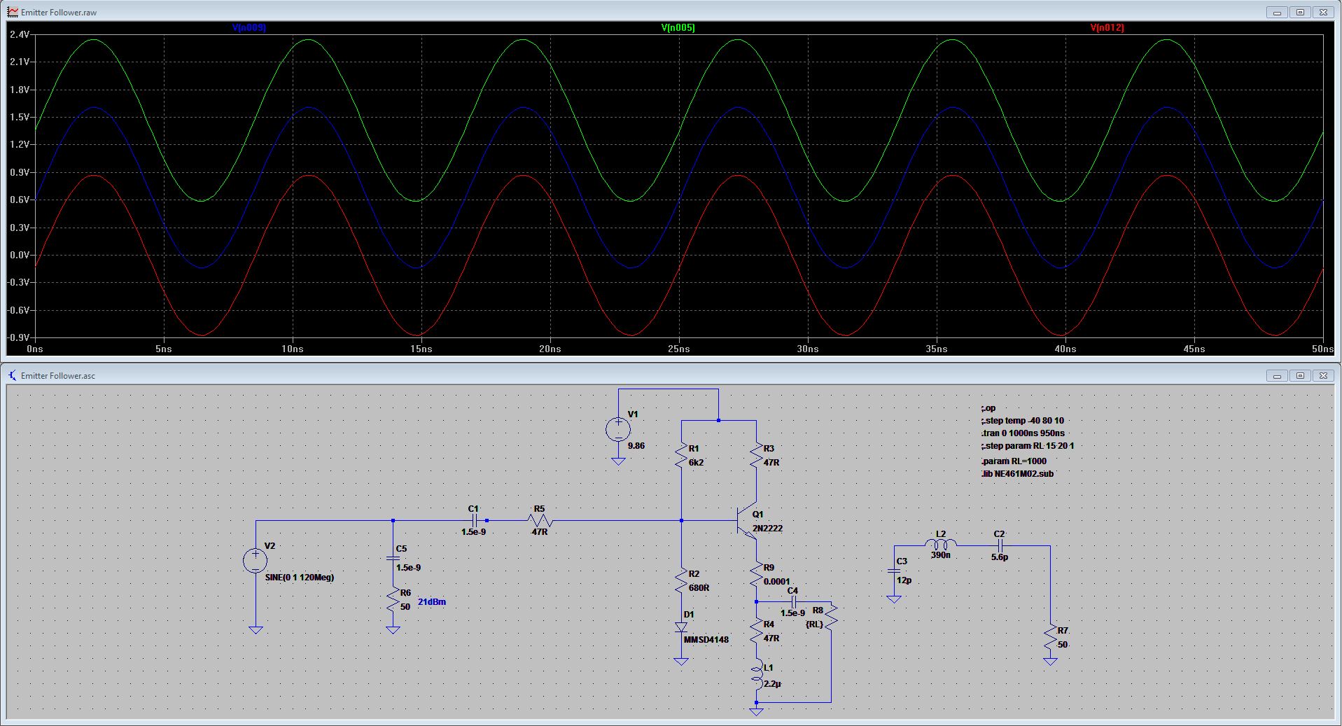
I have simulated the attached emitter follower circuit in LTspice. Since the transistor is biased from a single postive supply, I don't understand how the output waveform (Red) can be going negative? Surely the waveform should be clipping when it goes below 0V? Note, the output is taken at R8.


Thanks
 

Attachments

  • Capture.JPG
    Capture.JPG
    276.1 KB · Views: 78

Because the coupling capacitor cannot transfer dc signals the output across R8 swings around 0 volts. That's quite normal. Why are you surprised?
 

Yes sorry I did realise I was being stupid after posting. I've been looking at this thing for too long!

But I do have another question about it. I have actually built the circuit, and in the real application the signal source (into this circuit) is coupled off from a 24dBm main signal. In this Spice circuit I have tried to replicate the fact that most of the signal power goes elsewhere by putting a 50Ohm load resistor R6 on the input. So a small amount of power arrives at the base of this emitter follower which is required to generate 13dBm across the load of 50Ohm.

In the real circuit when I measure the output on a Spectrum analyser I do indeed get 13dBm. Great. But when I look at the output using an oscilloscope set to 50Ohm input impedance, the voltage waveform I get is 4V amplitude, which corresponds to 22dBm in 50Ohms.

I don't understand why there is this difference?
 

R6 and C5 have no effect in your simulation circuit, because V2 is an ideal voltage source. This setup will be hardly found in the real world, where generators have an output impedance, usually 50 ohms.

As an additional point, I don't expect that the used 2N2222 model is modelling the behavior at 120 MHz accurately, also your simple simulation circuit doesn't take account for package inductance and similar parasitic elements. In so far differences between simulation and real measurement won't be surprizing.
 

Thanks. Ok, I see your point regarding the source. In the real application the source is in fact a common base stage which delivers about 24dBm to a 50Ohm(ish) load. A small amount of power is then coupled off from the output of the common-base stage to drive this emitter follower.

How would I best be able to model this real signal source in this simulation? I know that the collector output of the CB stage should be relatively high impedance with a 50 Ohm load in parallel with it.
 

I don't understand "small amount of power" because there's no attenuator. At best it's -6 dB (50:50 ohm). The real source can be modelled as a voltage source with series or a current source with parallel resistor, they are equivalent.
 

A oscilloscope isn't a 50Ohm resistive load but more of an impedance. In other words it might be different for different frequencies. I had a similar problem assuming a resistive load in a high frequency environment.
 

Status
Not open for further replies.

Similar threads

Part and Inventory Search

Welcome to EDABoard.com

Sponsor

Back
Top