Welcome to our site! EDAboard.com is an international Electronics Discussion Forum focused on EDA software, circuits, schematics, books, theory, papers, asic, pld, 8051, DSP, Network, RF, Analog Design, PCB, Service Manuals... and a whole lot more! To participate you need to register. Registration is free. Click here to register now.
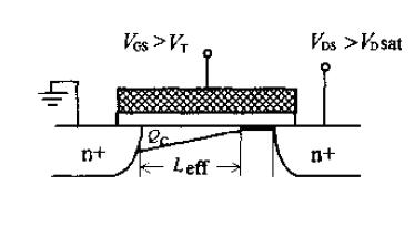
When VDS increased larger than VDSsat, its channel is pinched off, and there is the region of depletion between drain-channel. However there is also electric field(E) so the charge can pass the depletion region pushed by E.[/quote]
Hi,
As you have said Vds>Vgs-Vt, so there is no channel, but the field is so strong that the drain region extends to the source, and under the influence of drain voltage the carriers cros the channel and are collected at the drain.
on a more physicall approach you can say that the electrons from the current flow, actually "jump" from the doped region to the channel, 'pushed' by the electric field (Vds) applied between the n+ doped regions.
This site uses cookies to help personalise content, tailor your experience and to keep you logged in if you register.
By continuing to use this site, you are consenting to our use of cookies.