Continue to Site

Welcome to EDAboard.com

Welcome to our site! EDAboard.com is an international Electronics Discussion Forum focused on EDA software, circuits, schematics, books, theory, papers, asic, pld, 8051, DSP, Network, RF, Analog Design, PCB, Service Manuals... and a whole lot more! To participate you need to register. Registration is free. Click here to register now.

Why are N and P channel complementary Mosfets output waveform deviating from desired response?

Status
Not open for further replies.

jimmykk

Full Member level 3
Joined
Oct 2, 2014
Messages
158
Helped
0
Reputation
0
Reaction score
1
Trophy points
1,298
Activity points
2,863
N and P channel complementary Mosfets output waveform deviating from desired response

Hi

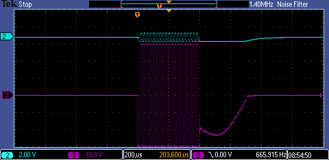
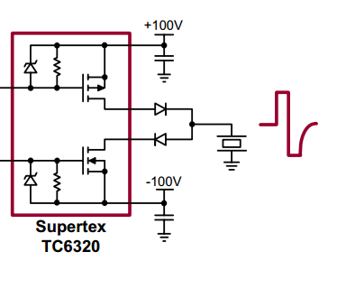
I am trying to make a pulse using circuits MD1213 and TC6320. The outputs obtained at drain terminals of MOSFET(TC6320) pair is not coming out as expected.i.e. basically the last negative cycle of the pulse takes a lot of time to return to zero(as shown in fig. CAHNNEL 3). I have provided voltages of +/-30V to source terminals of TC6320 and frequency of pulse is 50Khz. What could be the cause of this deviation and how it can be overcome.


Re: N and P channel complementary Mosfets output waveform deviating from desired resp

Post a schematic.
 

Re: N and P channel complementary Mosfets output waveform deviating from desired resp

I presume both transistors must be off to allow return to zero. How do you expect fast return in this situation? There must be either a short switch or a low-impedance load to achieve this.
 

Re: N and P channel complementary Mosfets output waveform deviating from desired resp

Hi

Here is my Schematics for Mosfet pair. If you check the datasheet(TC6320), You will see the output takes some time to go to zero from its peak negative value. What could be the possible reason for this behaviour.


Re: N and P channel complementary Mosfets output waveform deviating from desired resp

The waveform is as expected, see my previous post. After the pulse train, both transistors are off, the transducer is slowly discharged by the oscilloscope probe.

I don't see a particular reason why you would need to discharge the transducer fastly. The situation may be different for a transducer that is also used as receiver, but your schematic doesn't show a connected receiver channel.
 
Re: N and P channel complementary Mosfets output waveform deviating from desired resp

Your schematic shows D3 and d4 connected backwards if you are trying to feed negative power to S1 and feed positive power to S2.
If you showed plus and minus power at the connector on the schematic then it is obvious that the diodes are backwards.
 

Re: N and P channel complementary Mosfets output waveform deviating from desired resp

Place 10kohm/1W resistor across transducer and look if waveform is closer to what you expect.
 

Re: N and P channel complementary Mosfets output waveform deviating from desired resp

Your schematic shows D3 and d4 connected backwards if you are trying to feed negative power to S1 and feed positive power to S2.
@audioguru yeah these diodes were already changed as they should be. I forgot to change it in the schematics.
 

Re: N and P channel complementary Mosfets output waveform deviating from desired resp

Far better to use a full bridge with shunt to ground to provide low RdsOn for 3rd state of tri-level driver, with controlled guaranteed dead-time during commutation from +100 to -100 or alternatively switch to ground between commutation with floating dead-time between states of low RdsOn at V+,V-,0V. All depends on RC time-constants of FET and load.
This would be surely done if shorting the transducer is a design objective.

But apparently it isn't in the Supertex application circuit linked in post #4. The diodes have been supplement to allow free wheeling of the transducer, either during receive intervals in a bidirectional transducer toplogy, because multiple voltage levels are combined as in the Supertex demo board, or simply to alow a transducer swing beyond the rails.https://datasheet.octopart.com/MD1711DB1-Supertex-datasheet-11839677.pdf

jimmykk didn't yet explain why he wants fast decay of the transducer voltage. In the usual TC6320 applications it's not intended.
 

Re: N and P channel complementary Mosfets output waveform deviating from desired resp

@FvM I was just worried about the pulse duration of the pulse train.....because what i think is it...if pulse takes a longer time to settle down to zero than deisred, won't the pulse duration will be affected and thus range resolution.
 

Re: N and P channel complementary Mosfets output waveform deviating from desired resp

if pulse takes a longer time to settle down to zero than deisred, won't the pulse duration will be affected and thus range resolution.
Due to the resonant transducer behaviour, the slow pulse decay doesn't show in the transmitted soundwave.
 
Status
Not open for further replies.

Part and Inventory Search

Welcome to EDABoard.com

Sponsor

Back
Top