oneoldude
Junior Member level 1

- Joined
- Aug 12, 2013
- Messages
- 16
- Helped
- 0
- Reputation
- 0
- Reaction score
- 0
- Trophy points
- 1
- Location
- Florida, USA
- Activity points
- 257
I have been reviewing web posted discrete designs for output buffers for headphone amplifiers.
For discrete circuits it seems there is an overwhelming favorite. It is the Diamond buffer. I cannot see why it is favored over the common Complementary Symmetry PP topology. Perhaps someone can explain.
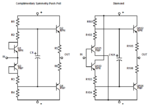
The schematic below shows two common, simple but functional versions of the two buffers.
The cap in each circuit is as suggested by Jung and in my simms that cap does a great job at reducing distortion in Class A mode. If either circuit will spend considerable time in Class B, an additional cap can be placed from the top of R5/R105 to the bottom of R6/R106. This will improve distortion in the Class B region. I do not want to go there so I have not included those caps.
It seems to me that the CSPP is better suited for discrete construction. Thermal feedback in the CSPP is between identical transistors, NPN to NPN, PNP to PNP. They are easy to match for diodic equivalency if you wish and of course the bias of the drivers is set by the diode junctions of identical transistors that are thermally connected.
The Diamond on the other hand has its output transistors biased by unlike transistors, NPN to PNP and PNP to NPN. These are much harder to match if you wish. Also, I have seen Diamond circuits on the net where the thermal feedback is NPN to NPN and PNP to PNP which makes no sense to me because the thermal feedback is not directed to the actual transistor that provides bias to a given output transistor. Indeed, I have seen circuits where the current in the bias transistors significantly exceeds the current in the outputs (a bit much if you ask me even for a current mirror) and each transistor is on a separate HS with no thermal feedback at all.
Am I missing something? What is it that makes the Diamond circuit favored over the CSPP in discrete designs? Is it higher and stiffer input impedance? Or is it the name?
I have simmed both circuits and both result in all distortion products down more than 120 dB with outputs biased at 25 mA and the buffer inside the feedback loop. The Diamond is a couple dB better though. As far as I can see they are virtually identical. With 25 mA Ic in the outputs, and a supply of +- 9V or more, it seems both circuits will supply sufficient current and voltage to fully power headphones with impedances from 30 to 300 ohms before crossing to Class B mode with low impedance phones. I know that a sim beggs reality but I am comparing apples to apples.
So, my two questions:
1. Why the Diamond buffer over the CSPP in a discrete design?
2. Shouldn't the temp compensation in a discrete Diamond be from bias transistor to output transistor NPN-PNP for proper temp stability?
Well, here are the example circuits and thanks for any help you can give.


