Continue to Site

Welcome to EDAboard.com

Welcome to our site! EDAboard.com is an international Electronics Discussion Forum focused on EDA software, circuits, schematics, books, theory, papers, asic, pld, 8051, DSP, Network, RF, Analog Design, PCB, Service Manuals... and a whole lot more! To participate you need to register. Registration is free. Click here to register now.

which one among the two will be fastest??

Status
Not open for further replies.

balavinayagam

Member level 3
Joined
Feb 24, 2010
Messages
59
Helped
9
Reputation
18
Reaction score
8
Trophy points
1,288
Location
banglore
Activity points
1,630
hi all!

this was a question that i got in my interview. i do not know the exact answer.
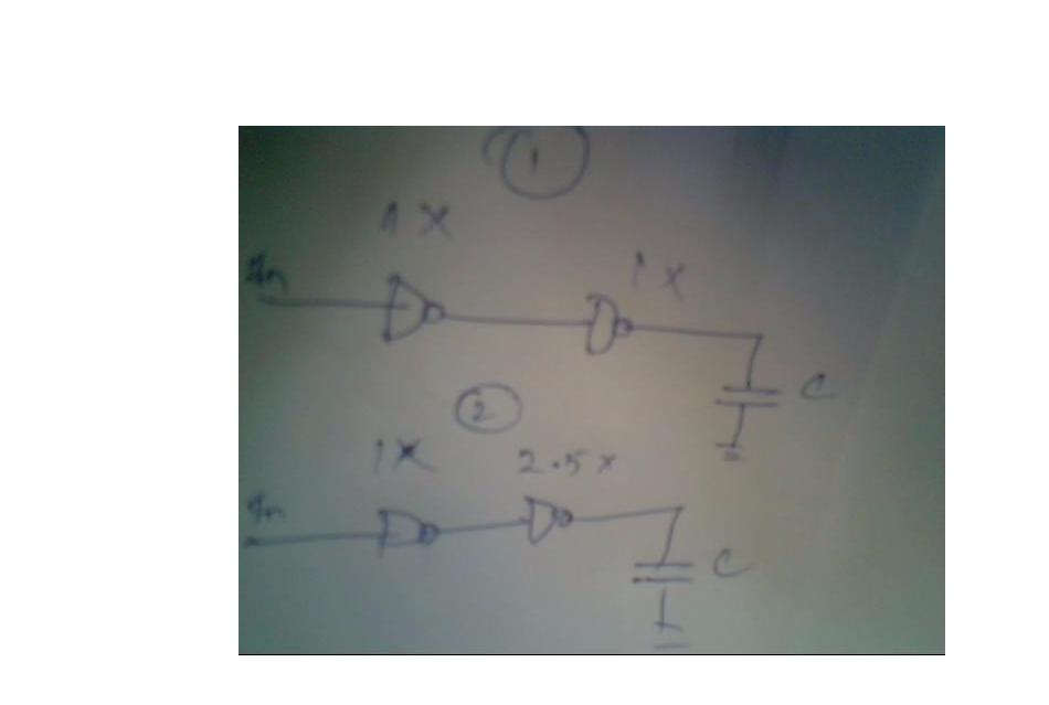
which one will be the fastest among the two??

what is that 1X or 2X denote-the amount of cap loading or its sizing?
pls clarify this

thanks in advance

---------- Post added at 21:56 ---------- Previous post was at 21:56 ----------


plz refer VLSI text books...................
 

I guess it is the propagation delay to cross the inverter. :)
 

Last edited:
X1, X2 etc. are drive strengths if following the standard convention that we usually use.

Which one is faster is difficult to answer from that pic. Higher X means higher input cap, but on resistance is smaller. Lower X is opposite. But I'd say the 2nd is most probably faster to charge/discharge the capacitor.
 
Lets make an assumption: the delay for each stage be RC where C is only the load.
For the first circuit: delay1 = Rinv*Cinv + Rinv*C
For second circuit: delay2 = Rinv*2.5*Cinv + (Rinv/2.5)*C

If you equate the two delays it will give a critical value of C which is 2.5*Cinv.

Hence delay for ckt 1 is smaller for C < 2.5 Cinv and larger for C > 2.5*Cinv. Both circuits will have equal delay for C = 2.5*Cinv
 
thanks nitin

but still i am not very clear..Pls post references or links

thanks all
 

A more precise computation:

Delay of any stage is the product of the resistance of the device and the sum of self and load capacitance. Generally the PMOS and NMOS of an inverter are sized to have equal resistance. Hence rising and falling delays are equal.

Circuit 1:

stage I: resistance = Rinv; capacitance = drain capacitance of first inverter + gate capacitance of second inverter. Assume Cgate = Cdrain. Then,
delay1_stage1 = Rinv*2*Cgate (since Cgate + Cdrain = 2*Cgate)
stage II: resistance = Rinv; capacitance = Cgate + C (here C is the load shown in the problem statement)
delay1_stage2 = Rinv*(Cgate + C)

Total delay of circuit1 = delay1_stage1 + delay2_stage2 = Rinv(3*Cgate + C)

Circuit2:
Stage1: resistance = Rinv; Capacitance = Cgate + 2.5*Cgate = 3.5 Cgate.
delay2_stage1 = Rinv*3.5*Cgate
Stage2: resistance = Rinv/2.5 (since size is 2.5x) and capacitance = 2.5*Cgate + C
delay2_stage2 = Rinv*(2.5*Cgate+C)/2.5

Total delay of circuit2 = Rinv(4.5*Cgate + C/2.5)

Equating the delays of the two circuits, we get Ccritical = 2.5*Cgate

Hence delay for ckt 1 is smaller for C < 2.5 Cgate and larger for C > 2.5*Cgate. Both circuits will have equal delay for C = 2.5*Cgate
 
Status
Not open for further replies.

Part and Inventory Search

Welcome to EDABoard.com

Sponsor

Back
Top