karthickb3e
Advanced Member level 4
hi one and all!
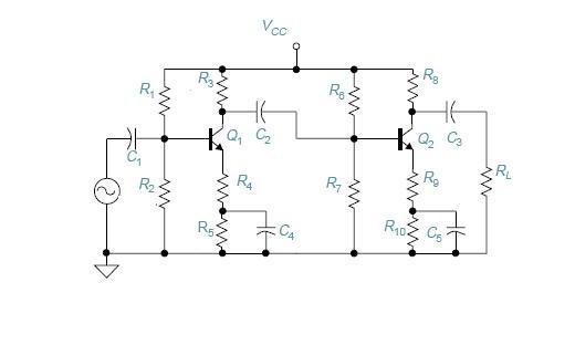
i need gain value of 1000. so i go for 2 stage amplifier ...... i got confusion in design references,
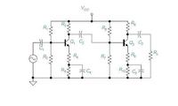
design 1
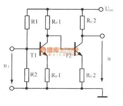
design 2:
in design 1:
2 stage is also given additional bias using R6 and R7....
but in design 2:
2 stage is biased from 1 st stage output .....
my question is additional voltage divider bias on 2nd stage is important or not....
if not putting it, may be happen any other problems or not........ which design is better?
please help ...!
i need gain value of 1000. so i go for 2 stage amplifier ...... i got confusion in design references,
design 1
design 2:
in design 1:
2 stage is also given additional bias using R6 and R7....
but in design 2:
2 stage is biased from 1 st stage output .....
my question is additional voltage divider bias on 2nd stage is important or not....
if not putting it, may be happen any other problems or not........ which design is better?
please help ...!
Last edited: