Continue to Site

Welcome to EDAboard.com

Welcome to our site! EDAboard.com is an international Electronics Discussion Forum focused on EDA software, circuits, schematics, books, theory, papers, asic, pld, 8051, DSP, Network, RF, Analog Design, PCB, Service Manuals... and a whole lot more! To participate you need to register. Registration is free. Click here to register now.

[SOLVED] Whether buffer amplifiers are needed or not in this circuit

Status
Not open for further replies.

d123

Advanced Member level 5
Joined
Jun 7, 2015
Messages
2,505
Helped
494
Reputation
992
Reaction score
525
Trophy points
1,393
Location
Spain
Activity points
27,148
Hi,

I can never tell if I use unnecessary buffers in the circuits I work through.

Question 1: Should buffers be used on all or any of the resistor string outputs 'a' to 'e' as they are supposed to be stable voltage references, and should two buffers be used for output 'e' as it is a reference voltage for two separate comparators (or op amps)? Or should they be perfectly fine without buffers?

Question 2: I saw this approach in an Analog Devices or Linear Technologies datasheet or app note - placing bulk capacitors around each resistor in a string to reduce noise/fluctuations in the output voltages. Is that a good approach to follow in the schematic in the picture?
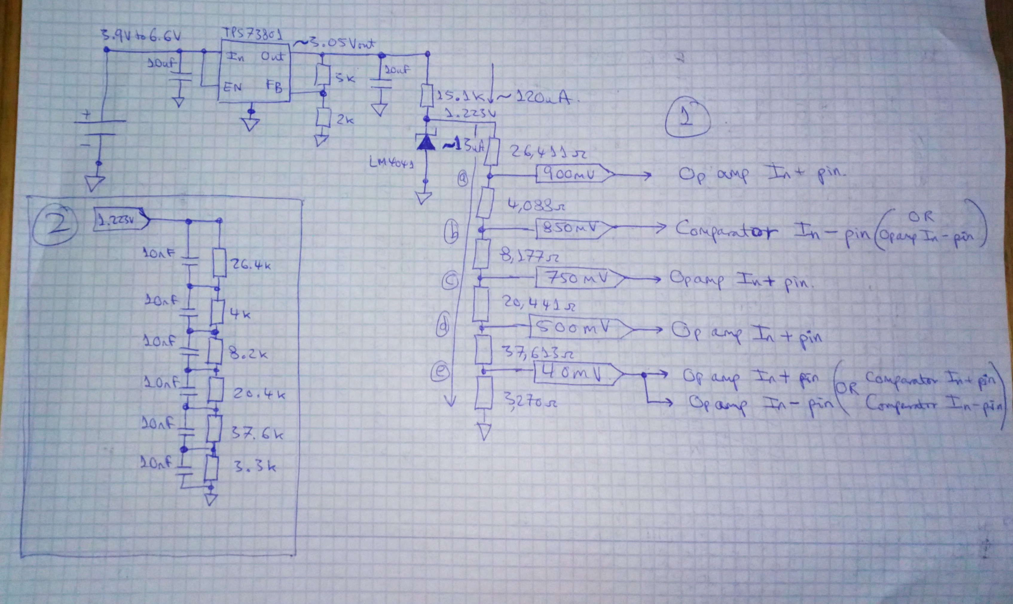
_20201021_213132.JPG


Thanks.
 

Ad 1. It is dependent to input impedance of block connected to such resistor tap. If it be capacitive only (CMOS gate with internal ESD) than buffer is not necessary. However, if you are planning to connect a guy who is sinking noticeable DC current from it, buffer is needed to avoid voltage drop at whole res ladder.

Ad 2. By adding cap to each res tap net, you will simply lower impedance for high frequencies and filter noise.
However, I would prefer to connect cap from tap to ground rather then parallel to resistors.
But, I am not a real electronic engineer, so might don't see something as well.
 
Comparators and op amps have such high input resistance (1M typical) that they do not load a signal very much. However if the signal comes through a high resistance, say 100k, then there is a 10 percent error caused by 1M input resistance.

Your series resistor stack approaches 90k total. It feeds several devices which might result in a loading effect. This falls into the category of fan-out error.

The bottom resistor is 3270 ohm. Whatever voltage appears on it, it won't be affected much by a 1M input resistance in parallel.
--- Updated ---

There are FET-input op amps which have extremely high input resistance, and do not substantially load a signal.
 
  • Like
Reactions: d123

    d123

    Points: 2
    Helpful Answer Positive Rating
Hi

Indeed it depends on your requirements. The rest can be calculated using Ohm's law.

If there is a source resistance/impedance of 3270 Ohms and you want it to be accurate to 5mV (example) then the current drawn from this node should be less than I = V / R = 0.005V / 3270 Ohms = 1.53uA. When there is a series resistor of 1M then the voltage across this resistor should not exceed V = I x R = 1.53uA x 1MOhms = 1.53V.

Klaus
 
  • Like
Reactions: d123

    d123

    Points: 2
    Helpful Answer Positive Rating
Hi,

Thanks for three very helpful answers. They provide very useful information that goes a long way to understanding both questions, the preferable capacitor connections/one bulk capacitor and how to calculate the answer to the buffer question. Great.
 

Hi,

One comment to the capacitors in parallel to the string - actually just

* the upper capacitor parallel to 26.4k:
I often omit it. Thus all high frequency noise is suppressed - even the noise of the source - the signals are all AC coupled to GND.
If there is the capacitor then you get the AC of the source to be divided in voltage divider manner since the capacitors are all connected in series.

* This is the next point... capacitors connected in series.
If you expect noise from the load, then a series connection is counter productive, since it spreads the AC noise via the capacitors to all other string nodes.
Then - connecting each capacitor to GND is an improvement.

It´s all a question of requirements, situations (schematic), PCB layout, noise sources.....and sometimes personal taste.

Klaus
 
  • Like
Reactions: d123

    d123

    Points: 2
    Helpful Answer Positive Rating
Hi,

Yesterday I calculated for 1mV error at each node/tap ('delusional' 1mV error per node is because I expect the error to be much worse in reality so it must be wiser to aim as high as possible to end up less low that desired(?), not because I think it is attainable in my hands). That was okay, as far as I've understood your answers, as the results are above LMC6464 input current of 10pA max. and offset current of 5pA max. and input resistance at 5V DC says 'Tera Ohm'.

LM35 takes 40us to settle to final value at 20ºC, 5Vsupply and 0.2Vout - Inverting amplifier node d ref of 500mV and node c clamp ref of 750mV are related to this, so should be as fast or faster to reach settling time. Another part of circuit needs the node e 40mV reference at power-up as soon as possible. When I turned to calculating tau for the resistive divider with 100pF, 1nF, 10nF and 100nF to see which best fitted my needs, I think my calculations are wrong of e.g. node a tau= C1 * R1; node b tau = C2 * (R1 + R2), etc.

The results I got for 5 tau with 100pF bear little relation to the simulation results. Apologies for piece of paper with my calculations. I see regarding C selection that it's another 'hard-to-choose with two opposing requirements' thing: 100pF is a fast start-up but fC is huge, 100nF is too slow with far more preferable fC... I chose start-up time over fC as it seems more important to circuit operation.

I haven't yet found any online resources that explain how to calculate the taus for n-order low-pass filters, all I've found are multiple examples of calculating nth-order LPF fC & f-3dB & slope and gain, but no tau.

Does anyone know how to calculate each tau or the general rule-of-thumb to estimate when e.g. node e (40mV) would reach it's 5 tau value? Are they all consecutive or staggered due to rise time of each preceding stage?

PC LED TORCH RDIV RC START-UP TIMES V1.JPG


PC LED torch Rdiv RC start-up times my calculations.JPG


Thanks.
 

Hi,

I don´t understand.
Why do you want the nodes to be "fast"? I thought them as DC reference... and here the slower the less noise, the better the precision.
I´d add at least 100nF maybe 1uF. But I don´t know your requirements regarding speed.

Do you want the LM4041 to continously switch ON and OFF? What timing?

What does "...40mv as soon as possible..." in time?

And yes, they all are staggered low pass filters.

For sure there are many ways.. Each node may have a separate voltage divider (instead of a string).
Then each node is independent of the other and may be independently adjusted in voltage and settling time.

Klaus
 
  • Like
Reactions: d123

    d123

    Points: 2
    Helpful Answer Positive Rating
Hi Klaus,

Thanks very much.

Hi,

I don´t understand.
Why do you want the nodes to be "fast"? I thought them as DC reference... and here the slower the less noise, the better the precision.
I´d add at least 100nF maybe 1uF. But I don´t know your requirements regarding speed

I don't want them to be fast. DC would be ideal. I thought I need the voltage reference and its taps stable before the op amp clamps or CCS op amp do anything undesirable like swinging to the positive rail until their reference voltages reach their final value.

I would have preferred 100nF or even 1uF myself, too, but think I need the reference voltages stable before anything else at start-up and at latch power-up of those sections. Maybe I'm completely wrong about that.

What benefits are there with 1uF over 100nF?

My newbie reasoning: I ended up with two versions of that torch circuit: v1 is the basic version and v2 has a shutdown section and a temperature-dependent voltage reference to limit LED current at higher temperatures. V2 is overkill for a 27mA torch, it's just to get the circuit right as I hope I might find the additional blocks useful for higher power applications with higher Iq and higher load/LED current. As you know, I learn little by little by exploring circuit ideas as they always force one to learn more about the sub-circuits, whether RC stuff, dividers, op amps, everything.

Do you want the LM4041 to continously switch ON and OFF? What timing

Only switching on and off for v2 E and F circuit blocks. LM4041 (block B) for the latch (block C) that controls blocks E, F, G, H and its 40mV tap within ~20us would be good. Block E, the LM4041 and its taps for the temperature-dependent voltage reference in less than 40us, ideally.

LM4041 says 4us settling time @ 25°C, 5V and 30k Rs (125uA for Iq and I load). Large signal response graph was more like 15us.

LM35 says ~40us @ 20°C, 5Vsupply, 0.2Vout. I am trying to get the 500mV, 750mV and the 850mV references stable/at their settled value before the LM35 stabilizes/settles - maybe that's not even necessary.

What does "...40mv as soon as possible..." in time?

For v1 and v2, asap 40mV means within ~20us. Maybe this is unrealistic and/or unnecessary.

And yes, they all are staggered low pass filters.

Thanks. I bet that's very hard to calculate. I'll sim-u-cheat my way to those answers for now.

For sure there are many ways.. Each node may have a separate voltage divider (instead of a string).
Then each node is independent of the other and may be independently adjusted in voltage and settling time.

Klaus

Great idea of separate strings, looks necessary for last-in-line 40mV refs as the capacitor drain section is delightful (it works well)... I think I prefer to do what you suggest as it would make start-up timing easier for me to figure out.

Then I imagine to keep - for example - 2 resistor string currents to e.g. the 12.23uA each of one 100k string at 12.23uA, I need to think of parallel resistors and make both strings 200k total each, and factor double the load current into the LM4041 Iq + I load calculations.

Maybe I'm being far too fussy over small details thst are beyond my technical ability on a pcb. And, I think my start-up/power-up and power-down timing lists are probably naïve and therefore wrong.

_20201023_174513.JPG
 

Some comparators can throw "kickback noise" out
the inputs (as well as into ground) when they switch.
It's good to minimize the driven load, for the ground
bounce (which will then travel through those "filter"
caps to the other side, inputs to various other devices).
Kickback noise is unlikely to be simulated properly by
behavioral models, or even by transistor-level if the
chip parasitics and things like shoot-through current
in the output stage are not captured in detail.

Deciding which ground domain the comparator(s)
ought to live in, is a design question (effects of output
nastiness, vs input nastiness from ground-ground
transient divergence, how's the HF PSRR look on
that comparator?).
 
  • Like
Reactions: d123

    d123

    Points: 2
    Helpful Answer Positive Rating
Hi dick_freebird,

Some comparators can throw "kickback noise" out
the inputs (as well as into ground) when they switch.

That's useful to be aware of. What kind of comparators/input structure, or is it random and hard to guage from datasheets?

It's good to minimize the driven load, for the ground
bounce (which will then travel through those "filter"
caps to the other side, inputs to various other devices).

Wow, thanks a lot.

Kickback noise is unlikely to be simulated properly by
behavioral models, or even by transistor-level if the
chip parasitics and things like shoot-through current
in the output stage are not captured in detail.

All Spice models are (usually) paragons of virtue with few blemishes... Anyway, an open collector like the LM193/LM2903 wouldn't have shoot-through, would it?

Deciding which ground domain the comparator(s)
ought to live in, is a design question (effects of output
nastiness, vs input nastiness from ground-ground
transient divergence,

So a comparator should be in power/switching transients section of a pcb, but as Klaus said, the comparator voltage references in a quiet part of the pcb and buffered? Does that mean using an op amp as a comparator from a quad package that has other op amps that need a quiet ground connection is a bad idea/a no-no?

how's the HF PSRR look on
that comparator?).

Would I find that in the datasheet (and hopefully understand it)?

The ...less bad I try to make my circuits, the more out of my depth I feel, and a bigger idiot who is a tiny thing lost in a city of huge copper tracks, invisible inductances, etc., things that happen I have no clue about, and capacitors and resistors whose complexities are like labyrinths with many levels each. A resistor ladder is a whole world in itself, add capacitors and there's weeks of study there. Really brings home how hard what you professionals do is and the scope of your learning.

Many thanks for the insights.
 

Hi,

There are lots of threads on kickback noise here on the forum, it's CMOS latch comparators - LM2903 is bipolar, so I guess it wouldn't apply to that IC.

Nice explanation in this thread.
 

Does anyone know how to calculate each tau or the general rule-of-thumb to estimate when e.g. node e (40mV) would reach it's 5 tau value? Are they all consecutive or staggered due to rise time of each preceding stage?
First order approximation is cap value multiplied by paralel connection of resistance connected to node (or more precisely from node to small signal ground, which means, that supply is a ground and large cap too).
However, with your RC ladder Elmore rule might work better.
 
  • Like
Reactions: d123

    d123

    Points: 2
    Helpful Answer Positive Rating
Hi Dominik,

First order approximation is cap value multiplied by paralel connection of resistance connected to node (or more precisely from node to small signal ground, which means, that supply is a ground and large cap too).
However, with your RC ladder Elmore rule might work better.

Thank you. I read a bit about Elmore delay - seems like I could actually do/understand the formula, great option.

What does 'supply is a ground and large cap too' mean, please?

I did the first-order approximation you explained, if I got it right, node e would take ~30us for tau and ~150us to reach 99.3%5 tau. Hope that's right. Simulation said about 90us to 100us, obviously would prefer the maths approach to endless zooming in to a simulated graph for an approximate answer, so thanks.
 

What does 'supply is a ground and large cap too' mean, please?
My "mind shortcut".
One of the principle of small signal analysis is to replace all source by their internal impedance, so voltage source is shorted to ground. This is rather easy to see, as on attached sketch:
Notes_201024_220318.jpg


The second part of my statement is related to impedance of large cap. It is less obvious, but we can ommit large cap or resistors shunted by large cap in some cases. Similar to case of analysis of degenerated common emitter amplifier with blocking Capacitor in emitter.
 
  • Like
Reactions: d123

    d123

    Points: 2
    Helpful Answer Positive Rating
Status
Not open for further replies.

Similar threads

Part and Inventory Search

Welcome to EDABoard.com

Sponsor

Back
Top