Continue to Site

Welcome to EDAboard.com

Welcome to our site! EDAboard.com is an international Electronics Discussion Forum focused on EDA software, circuits, schematics, books, theory, papers, asic, pld, 8051, DSP, Network, RF, Analog Design, PCB, Service Manuals... and a whole lot more! To participate you need to register. Registration is free. Click here to register now.

When Large Switch Transistor suddenly turn off, What Happen?

Status
Not open for further replies.

020170

Full Member level 4
Full Member level 4
Joined
Jan 31, 2005
Messages
231
Helped
3
Reputation
6
Reaction score
1
Trophy points
1,298
Visit site
Activity points
2,221
In CMOS Process, I designed Large NMOS/PMOS switch Transistor.

To protect switches from large Ids current, I designed protection circuit and inserted it.

It is supposed to operate when Ids current > 300mA , PMOS gate pull on(VDD) and NMOS gate pull down(GND). So Ids current doesnt flow any more.

On the contrary to concerns, when large current flow through NMOS switch, switch has no damage.

Rather after large current flow, -> protection circuit operate -> NMOS gate is about to pulling down, switch has damage.

I don't understand why NMOS switch has damaged when NMOS switch is about to turn off.

In my opinion, NMOS switch damage is relevant to latch up issue.

Is there any one who help me? I want to know inside knowledge about it.

Thanks.
 

A picture would be worth something.

You might be seeing something like the flyback of an
inductive load*, driving the NMOS past breakdown when
the current loop as-it-is is interrupted. Current in
normal conduction is diffuse. Current in breakdown is
prone to hot-spotting at the weakest point. The
output transistor design may want ballasting, the
drain contacts pulled back from gate and silicide
blocked in between to get a resistance that will fight
crowding. This costs you conduction, yes. But you
live to fight another day.

* Even if you think it isn't inductive, any wire length
adds some. And an ATE test head adds plenty. You
might assess this, make a lumped element load model
and try simulating the operation again, looking for any
voltage rating violations on the NMOS.
 

Thanks for your reply.

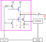
In my explain, I said "I designed MOSFET switch". Its operation looks like "switch", But It's not switch. It's BUFFER's output stage.

??1.png

PMOS/NMOS MOSFET is so large(Blue) , It can drive large current.

Red Voltage source is Test Voltage. It may be 18V.

When too much current flow, IR drop votage is generated by 400ohm resistor. IR voltage drop sensing block is sensing it, and protection signal is out.

I don't understand ballasting layout. What it the pros rather than conventional CMOS MOSFET layout?

Due to parasitic inductive elements, may be generated voltage caused by inductive characteristics. I will check this today.
 

Another problem to beware, at automated test, is the
"force current, measure voltage"approach. Even if you
properly set a voltage compliance limit, this can be too
slow to react to save the DUT particularly if the output
is in the wrong logical state. It acts like a flyback over-
voltage even though the root cause is not inductive per
se.

Hard-interrupting current in the PMOS, with some break-
before-make timing to the NMOS, is asking for this or
true flyback damage. You might prefer, for the short-circuit
case, a little bit of cross-conduction timing (why not, it's
already cooking, what will a couple of nS hurt?) so that the
current can never go to zero and swing the voltage hard,
high.

Ballasting's only "pro" is simple toughness. It mitigates
the tendency to concentrate current in the power switch.
You often will see this style embedded in library ESD
devices, but in my experience this can be "missed" in
PDK / standard cell pic-connected active devices. But
the exact same concerns apply to these, as ESD devices -
they share the same current loops after all, and you want
to do more than hope that the ESD device takes all of the
hit - but when the driver exceeds the size of the clamp,
and uses the same core device, this wishful thinking (if
it is thought about at all) fails, the driver becomes the
primary path for breakdown currents and therefore you
should apply the same thermal/electrical design methods
at the bottom level device layout.
 

Even a piece of wire can be classed as inductive because it has a property of inductance.
I checked this one but over voltage is not measured.

??3.png

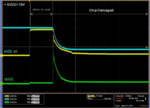
A1 is large PMOS/NMOS drain terminal. We set this output voltage as 0V.
AVDD=18V, IAVDD is AVDD current by measured current probe.
During about 1.5msec, AVDD & A1 is shorted. but damage is not happen.
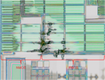
After about 1.5msec, damage is happen. chip is damaged, so I delayered.

??4.png

Damage point is on the border line between NMOS and PMOS.

I don't know what should I do for damage analysis.
 
Last edited:

Looks like latchup to me. Does adding capacitance on A1 prevent the chip from dying? For example, 1 or 10nF?

You should zoom-in on the turn-off transient (to about 20ns/div) to really be able to see if inductive ringing is killing your chip. And for V(A1), probe directly on the pin closest to the chip and use a really fast probe.
 
  • Like
Reactions: 020170

    020170

    Points: 2
    Helpful Answer Positive Rating
Thanks for your reply.

As you said, I added 10nF capacitor on A1 output, but the result is same(chip damage happened).
Next I added 47nF capacitor on A1 output. At this time, the result is different, chip is more robust to damage than no capacitance condition.

I don't know why more capacitance causes less damage. What is the relationship between latch-up and output capacitance value?

As you said, tomorrow I will check about turn-off transient to be able to see peaking voltage caused by inductive property.

Would you tell me about fast probe? Is it different comparing with normal voltage probe?

I really appreciate your help.
 

My current suspicion is that the parasitic inductance in the A1 path is storing energy, and when you turn the NMOS off, the inductance causes the voltage V(A1) to rise above V(AVDD). The PMOS body diode begins to conduct when V(A1) > V(AVDD) + 0.7V. A parasitic PNP+NPN SCR (which exists in your PMOS and NMOS) activates, causing a very high current to be drawn from AVDD, directly through your chip to GND until the devices break.

Adding capacitance probably helps by absorbing the inductive energy spike, and preventing V(A1) from rising above V(AVDD) + 0.7V. This is only helpful in troubleshooting what the problem could be; for a real fix (if the SCR is indeed the problem), you want to suppress the SCR through layout techniques.

Update:
As for fast probing, if you have a >200MHz probe you should be able to measure it; just take the probe's endcap off and use a short "pigtail" ground connection instead of the ground strap. See the Jim Williams app note, AN-47 for more info (see page 16).
 
  • Like
Reactions: 020170

    020170

    Points: 2
    Helpful Answer Positive Rating
Thank you for your reply.

Unfortunately, there is still a mysterious phenomenon that isn't explained with latch-up .

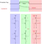
When opamp near-pin short issue is happen, short current flows through NMOS/PMOS and then protection flag signal is rising high. If short current is greater than 200mA for 100usec, protection signal is high for 100usec,too. After 100usec, protection flag turns to low and NMOS/PMOS switch turn-off instantly.

Detail timing diagram is below

a1.png

I controlled protection flag time from 127usec to 167usec. When I set up protection flag time at 167usec, chip is damaged and protection circuit does not operated normally.

a2.png

Damage looks like dependent upon protection flag time. Latch-up phenomenon is dependent on current-flow-time? Besides, current flowed through NMOS/PMOS transistor is not increased at time.

I don't understand why damage is dependent on protection flag time. Could you explain the reason?
 
Last edited:

Are you sure damage depends on flag duration, and not the
other way around?

What activity attends the protection flag release event? Is
this perhaps choking off some thermal rise before damage
accrues?

There's latchup and there's latchup. You can have chip scale
or localized, and you can have enough current to fry junctions
or interconnect, within some timescale (heat mass divided by
input power, against critical temperature rise). Some latchup
loops may be "modulated" by local logic / analog / switch state
(shunting, say, an insufficiently-tied-down parasitic base node).

You might find it amusing or instructive to watch the die under
a microscope (optical, or emissions) and see the location of the
hot spot - emissions microscopes, some at least, can even take
a little movie slaved to a trigger. Speculating based on your
intention & schematic design hasn't got all the pieces in place.
 
  • Like
Reactions: 020170

    020170

    Points: 2
    Helpful Answer Positive Rating
Status
Not open for further replies.

Similar threads

Part and Inventory Search

Welcome to EDABoard.com

Sponsor

Back
Top