Continue to Site

Welcome to EDAboard.com

Welcome to our site! EDAboard.com is an international Electronics Discussion Forum focused on EDA software, circuits, schematics, books, theory, papers, asic, pld, 8051, DSP, Network, RF, Analog Design, PCB, Service Manuals... and a whole lot more! To participate you need to register. Registration is free. Click here to register now.

What's the equation between Leff and tox in mosfet structure?

Status
Not open for further replies.

stackprogramer

Full Member level 3
Joined
Jul 22, 2015
Messages
181
Helped
0
Reputation
0
Reaction score
1
Trophy points
1,298
Activity points
2,668
whats equation between Leff and tox in mosfet structure?

tox is width of oxide ,leff=effective length of mosfet?
whats equation(relation) between Leff and tox in mosfet structure?
in variety technology like .5 um ,.25 um,.11 um .
please help me?:oops:
 

Re: whats equation between Leff and tox in mosfet structure?

Effective channel length Leff has no relation to tox, it is just a necessary correction of the drawn channel length Ldrawn offset due to mask/etch effect, s. e.g. **broken link removed**, p. 15:
Leff = Ldrawn + XL - 2dL
Ldrawn can be an arbitrary length value ≥ process size.
 

Re: whats equation between Leff and tox in mosfet structure?

hi,thanks for replay,but i think that
(capacitor in volume unit)Coxide=ebsilon/tox result cox=ebsilon* W*L*1/tox
where L is length of channel and W is width of channel.
i want to now in variety technology(.1 um,.5 um and so on)Is there a other relation between L and Tox????

- - - Updated - - -

my means that for example for a transitor Leff is 1 um and tox=22nm how we can select 22 nm or 50 nm???????other relation i need!
 
Last edited:

Re: whats equation between Leff and tox in mosfet structure?

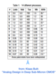
If you are willing to replace the arbitrarily long Leff (s. my explanation above) by Lmin , the min. length L allowed for a certain process, this table could help:
Relation_between_Lmin,Vdd,Tox,Vth,AVth.png
 
Re: whats equation between Leff and tox in mosfet structure?

thanks,this table where is? address of refrence ?
why for certaion tox,Lmin is limited??
how can i find the equations?

- - - Updated - - -

the article of klaas bult i finded but i have confused i should study and i soon replay
 

Re: whats equation between Leff and tox in mosfet structure?

this table where is? address of refrence ?
At the bottom of the table. Find it via G00GLE.
why for certaion tox,Lmin is limited??
Lmin is the min. structure size of a process technology allowed for transistor length L. This process uses a certain tox.
how can i find the equations?
Never seen such an equation - actually there is none. You could produce an approximate relation between Lmin and tox from the table values - at least for a limited range of process sizes.
 

Re: whats equation between Leff and tox in mosfet structure?

The relation is ad hoc, but driven by physical realities
(reliability at high fields, leakage / breakdown). The
relation is fuzzy because there are tradeoffs to be made
in vertical (gate ox) and lateral field distribution that
affect hot carrier and gate oxide wearout reliability, and
value judgements are made based on application, the
available equipment, and so on. The best you can do
is a foggy sort of correlation (and at the leading edge,
so few serious players that you must hold in mind the
possibility that the relation will change as the industry
matures at each node, over time - small sample size
at present, maybe (or not) broadening eventually).

Predictive equation, though? Fuggedaboudit.
 

Re: whats equation between Leff and tox in mosfet structure?

eq6x2_1.gif
i finally resulted this by relation above i.e. cox=ebsilon* W*L*1/tox
and relation Vth and this point that in design vth=.3 vdd
we can determine tox,in certain technology.

- - - Updated - - -

and we should attend to this point that limitation of gate oxide thickness
Limit of gate oxide thickness scaling in MOSFETs due … - ‎Koh - Cited by 54:
Meishoku Koh et al: "Limit of Gate Oxide Thickness Scaling in MOSFETs due to Apparent Threshold Voltage Fluctuation Induced by Tunnel Leakage Current", IEEE Transactions on Electron Devices, Vol. 48, No. 2. February 2001

A silicon nanocrystals based memory - ‎Tiwari - Cited by 1881
and the article that my friend erikl hints to,
it shows list table tox for many technologies
https://wenku.baidu.com/view/1959122ae2bd960590c677b9

my friends, thanks very much for your attention, if i get better result i will post another
 
Last edited by a moderator:

Status
Not open for further replies.

Part and Inventory Search

Welcome to EDABoard.com

Sponsor

Back
Top