Continue to Site

Welcome to EDAboard.com

Welcome to our site! EDAboard.com is an international Electronics Discussion Forum focused on EDA software, circuits, schematics, books, theory, papers, asic, pld, 8051, DSP, Network, RF, Analog Design, PCB, Service Manuals... and a whole lot more! To participate you need to register. Registration is free. Click here to register now.

What VDD and VSS means ???

Status
Not open for further replies.

AD76XYZ

Junior Member level 1
Joined
Jul 4, 2012
Messages
15
Helped
0
Reputation
0
Reaction score
0
Trophy points
1,281
Activity points
1,408
Hi,
Some times I saw in circuit VDD and VSS, here VDD means positive and VSS means zero. What is the full form of these VDD and VSS.
And is there any this type of three letter word for negative voltage and ground?

Any one explain in detail.
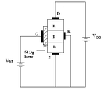
 

The microcontrollers has lots of mosfets inside of them. To make run a mosfet you should apply some voltages to its pins.
construction-type-of-enhancement-mosfet.png

Here a picture of mosfet.
Vdd= 'Voltage Drain Drain'
Vss='Voltage Source Source'
The Ground can be written in form of 'gnd'
 

    lucarlo

    Points: 2
    Hi tusemo, I am looking for help. I am wondering if you can talk about this, do you have any number or mail? Thank you
tusemo's right and on schematics and much older chips you'll sometimes find VCC or Vcc used. This meant 'Voltage Collector Collector' in a former BJT dominated world full of NPN and PNP transistors.

The double terms ('Collector Collector' etc) refers to a connection to that terminal side of many transistors, not just one transistor as per Vd/Vs/Vc etc.
 

BJT--- FET---"Vxx" meaning
________________________________
Vcc---Vdd |Positive supply voltage |
Vee---Vss |Negative supply, ground|
__________|____________________|

Apparently this terminology originated in some way from the terminals of each type of transistor, and their common connections in logic circuits (i.e., Vcc is often applied to BJT collectors, Vee to BJT emitters, Vdd to FET drains, and Vss to FET sources). This notation then carries across to integrated circuits -- TTL ICs were originally based on BJT technology, and so often use the Vcc / Vee terminology; CMOS ICs are based on FET technology, and so often use the Vdd / Vss terminology.
 
  • Like
Reactions: persibal

    persibal

    Points: 2
    Helpful Answer Positive Rating

    lucarlo

    Points: 2
    Hi Sherazi I am looking for help. I am wondering if you can talk about this, do you have any number or mail? Thank you
Hello!

Here a picture of mosfet.
Vdd= 'Voltage Drain Drain'
Vss='Voltage Source Source'
The Ground can be written in form of 'gnd'

This replies only partly to the question. Why voltage drain drain and not voltage drain only?

Dora.
 
its because you can have voltage between base and emitter that is called Vbe and so on so voltage at collector with reference to gnd is called as Vcc, and so ON

- - - Updated - - -

http://www.jestineyong.com/what-is-vcc-vee-vbb-vdd-and-vss-stand-for/
 
Thanks, that link explains it nicely. I had been wondering about this as well.

According to the article:
They are all supply voltages. Vcc = Collector supply voltage, Vee = Emitter supply, Vbb= Base supply voltage, Vdd = Drain supply, Vss = source supply.
[snip]
Since there is no notion to identify ground (0) this method was simply adopted. The voltages can be negative or positive depending on the the device and the circuit configuration. This method is a standard specified by Institute Of Electrical And Electronics Engineer (IEEE).
Assuming that's true, it's got to be one of the silliest decisions the IEEE ever made, IMO. According to the "standard", both supply rails in the circuit below should be labeled "Vss".


It was probably decided before CMOS - with NMOS only processes. It could have been said that VSS could mean 'substrate' but the first processes I worked on had an N type substrate so that wouldn't apply so I guess 'source' makes sense.

Keith
 

It is nice to know about these terms. The link provided by sherazi is really nice and informative. Now I understand the things. Thanks for helping me.
Thanks.............
 

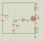
mosfet.JPG
Here I labeled every voltages in a basic circuit. The reason why it is called Vdd inside of Vd, is to make a difference between them, because they refer to different voltages in the circuit.
tusemo
 
Hello!

Here I labeled every voltages in a basic circuit. The reason why it is called Vdd inside of Vd, is to make a difference between them, because they refer to different voltages in the circuit.
tusemo

You're the first explaining why these double letters.

Thanks!

Dora.
 

Status
Not open for further replies.

Similar threads

Part and Inventory Search

Welcome to EDABoard.com

Sponsor

Back
Top