Continue to Site

Welcome to EDAboard.com

Welcome to our site! EDAboard.com is an international Electronics Discussion Forum focused on EDA software, circuits, schematics, books, theory, papers, asic, pld, 8051, DSP, Network, RF, Analog Design, PCB, Service Manuals... and a whole lot more! To participate you need to register. Registration is free. Click here to register now.

What is the use of connecting two parallel VIA2 holes in Agilent ADS ?

Status
Not open for further replies.

btv_murthy

Full Member level 3
Joined
Nov 29, 2011
Messages
159
Helped
9
Reputation
18
Reaction score
9
Trophy points
1,298
Location
BANGALORE
Activity points
2,719
Dear Sir,
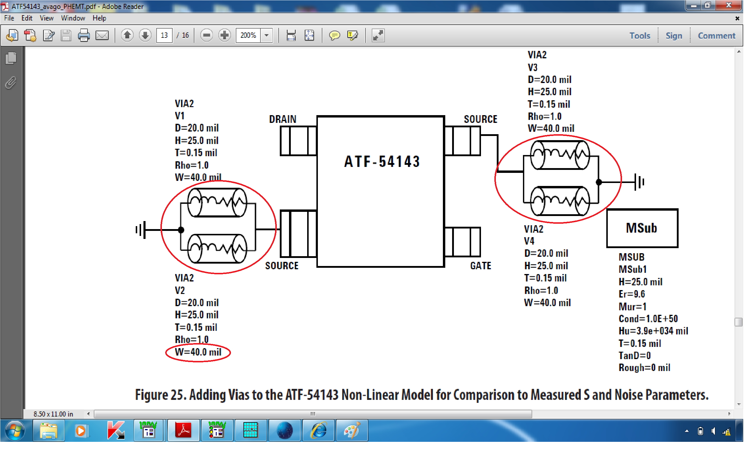
What is the use of connecting two parallel VIA2 holes ?. I have noticed in the datasheet of avago ATF 54143. What is the difference between the single VIA2 and two parallel VIA2 connecting. If we use the two parallel VIA2 connecting, will it not occupy more space in the board. In the VIA2 , W= width or diameter of the via pad, what is this?


ATF54143 is a p-HEMT FET that has useful gain up to 6GHz.
The are two connections to the source, and the S-Parameter characteristics will have been measured up to a definite point (measurement plane) on the lead-package layout.
For it to work, it has to have very careful attention paid to grounding the source leads. The inductance in the vias is quite enough that, even with two vias in parallel, four in total, the series inductance in the source has to be modelled, because provides some feedback.
The feedback from via inductance is degenerative (negative) at lower frequencies, increasing stability, but being frequency dependant, gets out of hand at higher frequencies, messing with the stability.
Probably at 6GHz, 4 vias placed real close will be enough. If that were a 20Ghz FET, more elaborate vias, using thinner substrate might be necessary.

Do not skip over what you do with the sources connections to groundplane! It can have a profound effect on everything else. The S-Parameters you think you are going to have for the device will likely not be what is in the datasheet. They will be for the device on your layout with the vias there. Model or calculate it.
 
Dear Sir,
Can you anybody explain me in detail answer to my posting #1 query.
 

Status
Not open for further replies.

Part and Inventory Search

Welcome to EDABoard.com

Sponsor

Back
Top