Welcome to our site! EDAboard.com is an international Electronics Discussion Forum focused on EDA software, circuits, schematics, books, theory, papers, asic, pld, 8051, DSP, Network, RF, Analog Design, PCB, Service Manuals... and a whole lot more! To participate you need to register. Registration is free. Click here to register now.
Clockgating is regulating the propagation of clock into a particular block.. suppose let us thing that there is a macro in chip which doesnot have any work for a long time.. then propagating clock to that module is a mere waste of power(as clock has the highest no.of transitions from 1 to 0 and vice versa.) so we will try to stop the clock propagation to that module.. we will resume the propagation of clock when it is needed..i.e, when the block is in use..how to do that? this is what is called as the concept of clockgating.. take a two-input AND gate and fix one input to clock and other to clk enable or chip enable (Assuming clk/chip enable is triggered at logic high). then the output of the AND gate is clk only when chip/clk enable is high otherwise always logic 0. This is known as clockgating..
One disadvantage od clock gating is the moment it passes thru AND/NAND gate, it will be treated a general toggling signal and clock buffers will nomore be inserted in its path.. So it is always advisable to have a clock gate very near to the block to which you want to do clockgating so that no more buffers are required inbetween.
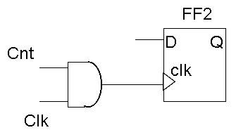
Clock gating is basically done to reduce the switching power of a flop. The circuit is like a flop in which its clock input is gated using an And gate. the other input to the and gate is a control signal. you can see in the figure. I don't think this changes the timing of the chip
first of all thankyou,
and i have one more doubt,that is how to decide the setup time of the clock gate(my design has TLATNTSCAX8)& tell about the noGating rising option
thanks
now the astro treats the clock gating path as a clock path only and not a signal path......so it adds clock buffers even in this clk gating path......after setting appropriate options in timing window......this was for synopsys tool....
for the question .. "how to deside the setup time of the clock gate"
This is just like a data path analysis..
Conside the same diagram posted by srkumar81... here compare with the ordinary scenario.. the clk pin for the gate is equivalent to the clk pin of the flop in general scenario and the "cnt" pin for the gate as the D pin for the flop in the general scenario...
So same rules apply for these clock gates as well...
A detailed discussion about clockgating or otherwise called as clock on demand,
and what all to be taken care, what will be the advantages is discussed
This site uses cookies to help personalise content, tailor your experience and to keep you logged in if you register.
By continuing to use this site, you are consenting to our use of cookies.