Welcome to our site! EDAboard.com is an international Electronics Discussion Forum focused on EDA software, circuits, schematics, books, theory, papers, asic, pld, 8051, DSP, Network, RF, Analog Design, PCB, Service Manuals... and a whole lot more! To participate you need to register. Registration is free. Click here to register now.
If I am not wrong then you can not comment on the delay of a circuit just by looking at the technology because delay of circuit depends on a lot of parameters namely current burned, MOSFET size, I/P signal slew and O/P load capacitor. You can have same delay in a 130nm ckt as in 90nm ckt if the above factors are properly manipulated.
But in general delay should be less in 90nm .... but a fixed value for it should be hard to comment ... If you can specify your target delay then we can suggest whether 90nm will work or not ...
Hello Dear Friend
thank u very much
yes, the amount of delay in a delay element depend on different parameter, but i want to know the minimum delay of a simple buffer.
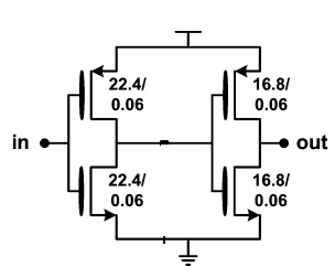
a simple buffer constructed from 2 inverter :
i saw in a reference that minimum delay for buffer in 65 nm is 20 ps.
but i work in 90 nm and this amount is important in my simulations and related results
i analyzed it with cadence and hspice and naturally with different W/L, we have different delay.
i found that lowest delay for 90 nm is 24 ps.
but i found in a reference that minimum delay in this technology is 40 ps and it's not possible to have lower delay !
(amounts of W/L in that image is just an example)
As we don't know about the reference that you have followed it would be difficult to judge in what context they have mentioned 40ps.
If the simulation results are 24ps then it is 24ps. BUT do check your load capacitor. About sizing I would like to say that the general practice is to keep PMOS size = 2 or 3 times NMOS size (depending on the mobility ratio in that technology). This gives the trip point of the buffer at VDD/2 (approx). But you are free to choose any size if trip point voltage requirement is higher or lower.
thank u very much dear friend
i saw in this reference:
L. Vercesi, A. Liscidini, and R. Castello, "Two-dimensions vernier time-to-digital converter," Solid-State Circuits, IEEE Journal of, vol. 45, pp. 1504-1512, 2010
that minimum delay for 65nm is 20 ps, but unfortunately i couldn't find that article that mention it for 90 nm
This site uses cookies to help personalise content, tailor your experience and to keep you logged in if you register.
By continuing to use this site, you are consenting to our use of cookies.
")