Continue to Site

Welcome to EDAboard.com

Welcome to our site! EDAboard.com is an international Electronics Discussion Forum focused on EDA software, circuits, schematics, books, theory, papers, asic, pld, 8051, DSP, Network, RF, Analog Design, PCB, Service Manuals... and a whole lot more! To participate you need to register. Registration is free. Click here to register now.

What is standard copper thickness for MCPCB?

Status
Not open for further replies.
T

treez

Guest
Hello,
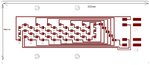
We are doing an MCPCB with 42 2W LEDs on it.
The LEDs have 700mA in them.
Is it normal to use 2oz copper (70um) with this?
I mean, with the copper being effectively heatsunk, you would think one ounce copper (33um) would be fine?
 

How large is the PCB (dimensions)? How long are the longest circuit etch traces and how wide?

If every LED is dissipating heat at the same time, a small PCB will get quite warm if it doesn't have something to transfer some thermal energy to?
Is this mounting on metal posts, or any kind of heatsink on the back side? If so, the heavier 2oz copper will spread the heat energy more effectively to a heatsink and I would choose that.
If the PCB has no heatsink to work with (it is its own heatsink) , the 1 oz copper will likely do OK as it can only radiate over so much surface area, and I assume the LEDs are distributed across the surface so one area doesn't have dramatically more heat to dissipate than another area.
 

Here is the LED MCPCB layout (top copper). Do you agree that there is no need for any topcopper pours on MCPCB?...after all, the heat is pretty quickly passed through the microscopic dielectric layer of the MCPCB down to the aluminium of the MCPCB.
 

Attachments

  • LED MCPCB.jpg
    LED MCPCB.jpg
    110.5 KB · Views: 175

I don't think that a top copper pour will help to any significant degree.
What dielectric material are you planning to use?

About 10 years ago I did some high power amplifier work where I used the TCLAD process/materials from Bergquist. Their HT dielectric was the best they ahd at the time, and it worked quite well.
I ended up with a copper substrate instead of Al because I really needed to spread the heat evenly to the available heatsink. The power MOSFETs (Switching at 100KHz) were mounted on a PCB about your size and when all was going at full power there was almost 200W power dissipation in that assembly. I see that Bergquist has a new dieletric available now for lighting applications like yours, I think:
https://www.bergquistcompany.com/thermal_substrates/dielectrics.htm

https://www.bergquistcompany.com/pdfs/T-Clad%20Optimal%20Design%20White%20Paper.pdf

In my MCPCB, I used 2 oz Cu as I had peak currents over 10A, and the heavier Cu also helped with my impedance matching. I think that 1oz Cu on your traces will be OK for those lengths at under 1A, just make sure you comply with trace width/copper weight requirements for the MCPCB materials/process that you've chosen.
 

thanks, do you know what is the minimum trace width acceptable for standard MCPCB likemy above in post #3
 

They are generally just a little more conservative than traditional FR4 fabricators, so probably 6-8mil minimum width on 1oz Cu is pretty safe. You have plenty of room on your layout so it looks like 15 or 20 mil on your pcb?
The 2nd PDF link in my previous post has design guidelines for the Bergquist processes toward the end of the PDF that may help as far as general clearance/holes, copper weight, etc. etc. Usually if you don't push the limits of one of these vendors then the design can be moved to others without too much hardship.
 

thanks, yes i have 0.3mm trace width throughout

- - - Updated - - -

For the MCPCB board in post #3, when the PCB manufacturer gets it out of the stores, is it initially totally covered in copper cladding?...which they etch away to give the circuit pattern?
 

Metal Clad process vary by manufacturer, and by board construction ( insulated metal substrate, double layer IMS, double sided FR4 with metal core, etc) and they have their proprietary steps.
The PDF at this link gets into various types of manufacturing steps used in several types of stackups, but it isn't exhaustive. It should give you plenty of information that would take too long to type here.

https://www.ncabgroup.com/wp-content/uploads/2015/10/07-NCAB_Group_Seminars_IMS_2_0_150930.pdf

I hope that this thread has been helpful for you.
 

The boards should be all copper, with just spaces for clearance. I would also look how the strings are laid out to avoid the long skinny tracks, that lay out looks all wrong for an LED board.
 

The boards should be all copper, with just spaces for clearance.
Thanks, is that so the copper doesnt peel off due to thermal cycling?
So what you are saying is it needs massive copper pouring?
Is there a limit to how big the clearance can be?
Why are "gaps" between copper not allowed on MCPCB?

- - - Updated - - -

The tracks outside the LED bank need to be skinny so that they don't go too near the screw holes.

- - - Updated - - -

I can understand there needing to be loads of copper pour on FR4 LED boards for thermal reasons...but surely on MCPCB with just 100um between the copper tracking and the aluminium substrate, surely the copper pouring is not so needed?
 
Last edited by a moderator:

The boards should be all copper, with just spaces for clearance. I would also look how the strings are laid out to avoid the long skinny tracks, that lay out looks all wrong for an LED board.
Thanks, i took your advice and put loads of copper pours connected to the LED pads...as attached. (Even though this is an aluminium PCB with just 100um of dielectric
between the led pad and the aluminium.
As FvM said in another thread it will be worth doing.
How does it look now?

Eagle i find is brilliant for adding multiple copper pours all individually shaped in this way.
 

Attachments

  • Aluminium PCB with copper pours.pdf
    110.8 KB · Views: 191

Wonder why you are tapering the copper pour next to the thermal pad. The suggested footprint in the data sheet looks better considered.

Did you calculate the total trace resistance?
 
  • Like
Reactions: treez

    T

    Points: 2
    Helpful Answer Positive Rating
Post a schematic if you can and some explanation of the led positions...
 
  • Like
Reactions: treez

    T

    Points: 2
    Helpful Answer Positive Rating
Thanks, please find the schematic and layout
 

Attachments

  • LAYOUT___LED MCPCB.pdf
    115 KB · Views: 134
  • SCHEMATIC__LED MCPCB.pdf
    60.3 KB · Views: 161

So, you are passing 700mA through each of (3) strings of LEDs, and summing all those currents (2.1A) into the small trace and running through those small 0805 (0,125 Watt) resistors in series?
I think you have some more changes to make.

Understand that even "0" Ohm resistors have some resistance. Understand that with 2.1A flowing through these resistors, it will only take a resistor value of 0.03 Ohms and you will be above the rated maximum limit for the part and it will fail. The traces will also be significantly warmer. Even with the MCPCB thermal efficiencies, I would still choose my trace widths to be more appropriate for ~10C - 15C temp rise with FR4 at maximum ambient temp (which is also going to be higher with all the power dissipation going on). Need larger package resistors and wider traces where ever possible.

At least your connectors are suitably rated
 
  • Like
Reactions: treez

    T

    Points: 2
    Helpful Answer Positive Rating
Thanks, a zero ohm 0805 resistor could be as much as 30 milliohms?
 

It could be possible. Usually they are less resistance, but there are always tolerances involved. Parts may be perfect initially but incur small damage from installation/soldering.
Do you have a 6 digit DMM to check some?

Also, observe this data sheet, for example:
https://www.mouser.com/ds/2/315/AOA0000C84-947596.pdf
and more importantly, this one-which is a pretty high grade/reliable part from Vishay. Not that the max resistance of the 0 ohm resistors can be 20-30 milliohms in those size ranges.
https://www.vishay.com/docs/31017/rcwp99.pdf
So, if you consider the higher reliability part could vary by this much with normal production tolerance, what about a lower grade part? Could it be a little worse?
At least, if you change from 0805 to 1206 package, the maximum current from Vishay goes up to 3.2 A, which is well above your frequent 2.1 so it should not pose a problem.

On the panasonic lower grade part, the rated current for 0805 part is 2A for "jumper" - which is referring to the 0 ohm part. It is the smallest package size that has that rating in the table. Even the larger sized ones are rated for the same 2, though they will generally handle more power dissipation without destruction. As you are planning to run this thing with 2.1A fairly often, I think you may be pushing your luck, particularly with 0805 package. At least if you move up to 1206 size package, you double your headroom of allowable power dissipation in case a part isn't 'perfect'. You have all of these resistors in series, so the failure of any one of them will cause complete failure of the entire unit, and you multiply the possibility of failure by the number of resistors you put in the chain. Adding in the fact that this will be in a warm/hot environment when operating, I would personally use larger 1206 parts if I could. They also give the advantage of providing more room for running wider traces underneath (which can also add some heating to the resistors). Note in the datasheet for max power derating for temperatures above 70C (hopefully this won't get that hot, but you never want to be close to the edge if you can help it). This is my opinion, anyway.
 
Last edited:

Thankyou ftsolutions, your info was crucial
I searched the web and wikipedia says that a zero ohm resistor could even be 50 milliohms.

In fact , the leds we use could have 1.05A in them, and if each of the (now updated) jumper resistors was 50 milliohms, then thats 496mW in each of them. (3.15A^2 *0.05)

Thats just getting too much , and i am actually going to specify 10 milliohm sense resistors, as 500mW even in a 2010 is possibly going to damage it with it being mounted on MCPCB.

The attached is how it is now. Do you think the copper pouring is ok?
 

Attachments

  • LAYOUT__LED MCPCB.pdf
    109.6 KB · Views: 148
  • SCHEMATIC__LED MCPCB.pdf
    72.5 KB · Views: 151

Well, don't always believe everything you read on wikipedia... but it better to be conservative than reckless in this area. So now the maximum current is 1.05A per string? Or, is this the nominal value and it could be more? I always consider designing with a safety margin in mind. How big that margin is depends on various factors, but it never less than 15% on power or current.

Now, can you consider "unwinding" your board trace paths? What I mean is - not knowing any other details than what has been evolving in this thread - if I were laying out the circuits on this, I would first try to put emphasis on the return "leg" that must carry all the current after it is summed back out to the connector. I would try to route that first with the widest track possible and not put any jumpers in it. Then, I would work on routing the (3) incoming traces to try to minimize how many jumps were needed to get the (3) incoming power legs to their respective strings. I don't know what specific placements you need for specific strings, but it seems that it might be possible to do it with only 2 or 3 jumps instead of 5 - and each of these would have less than the full/total amount of current passing through them. If so, then you can probably go back to using ordinary 1206 or 2010 O-ohm resistors as well. Only if I could not accomplish this for some reason would I resort to having to do the "inside-out" jumpering here on this layout. Maybe that is the case for you, I don't know.

You don't indicate how far away from the edges/holes you have to keep the traces. But I would use as much of the available space for current traces as necessary. Just be mindful of keeping whatever clearance is needed for the fabricator between traces for the process and the copper weight - 10mils/ .11mm is as small a clearance as I would get if possible. And only neck down/reduce the trace widths where necessary.

Myself, I don't really see the need for the extra copper pours on an all metal substrate board like this - I needn't use them on a similar sized pcb with 3X the power dissipation as this, but it likely won't hurt any either. Your choice, I guess. Note - you will only be able to solder (or unsolder) these boards running them through a proper SMT reflow oven, or very carefully over a quartz heater with a topside iron/gun. The heatsinking ability of these boards is very impressive and will prevent you from doing anything with any normal soldering on the planet - just be advised.
 

Thankyou very much ftsolutions , you saved our board from potentially going dead.

Myself, I don't really see the need for the extra copper pours on an all metal substrate board like this

Thanks, I must admit my intuition tells me that the 75um of dielectric on the MCPCB is just too thin to have much of a temperature difference across it, even without extra copper pours.
With eg the following Bergquist MCPCB, the dielectric between the LED’s copper footprint and the aluminium beneath has a thermal resistance of 0.32degC per Watt, considering 1cm^2.

MCPCB datasheet (dielectric)
https://www.bergquistcompany.com/pdfs/dataSheets/PDS_HT_3mil_1113.pdf

Each LED has an area of approximately 2mm^2, so in other words, considering three Watts dissipation per LED, that means that the temperature of the LED’s pad will be 24 degrees hotter than the temperature of the aluminium. However, the 2mm^2 is the LED’s total area. –But the only area of the LED that has a significant role in temperature conduction is the LED’s thermal pad…..and this has an area of just 1.8mm*0.6mm. Considering that reduced area, the temperature of the LED’s thermal pad could be expected to be some 39 degrees hotter than the temperature of the aluminium beneath it. But It seems impossible to believe that a 75um thickness of dielectric could have a temperature difference of 39 degrees across it. It just doesn’t seem right.


If copper pours are added, then its difficult to say how that will reduce this temperature difference. This is especially because the thermal pad of the LED is the only pad worth attaching a copper pour to. The problem is that this thermal pad has an exterior “edge” of only 1.2mm in total to which exterior copper pour can be attached…..so how do you assess how easily the heat of the LED’s thermal pad can be conducted out of this thin channel to the external copper pour?

It all seems a bit hit and miss.

My intuition wants to tell me that the 75um of dielectric on the MCPCB will have at most a degree or two of temperature difference across it.

Post #7 of this thread gives calculations that suggest copper pouring on MCPCB’s is well worthwhile…
https://www.edaboard.com/threads/365763/
 

Status
Not open for further replies.

Part and Inventory Search

Welcome to EDABoard.com

Sponsor

Back
Top