ltkenbo
Junior Member level 1
I am an electrical engineering student at a university. I am designing a project with my teach which uses zigbee technology. I have designed one of our circuit boards and I don't know a lot about microstrip stuff and RF board design but I did my best. The zigbee is in the 2.4 GHz range and the microstrip from the balun to the antenna needs to have an impedance of 50 ohms (to match the balun output and antenna).
Anyways I will include 3 pictures. The first one is the original. We had this board made on a mill machine. I designed the microstrip for using thin ".031 board, it is .055" wide which with that thickness of board should be around 50 ohms. However when we had it made at the school they used thicker ".062 board. However, it seems to be able to actually transmit a good distance. All shown dimensions are in mils (thousands of an inch)

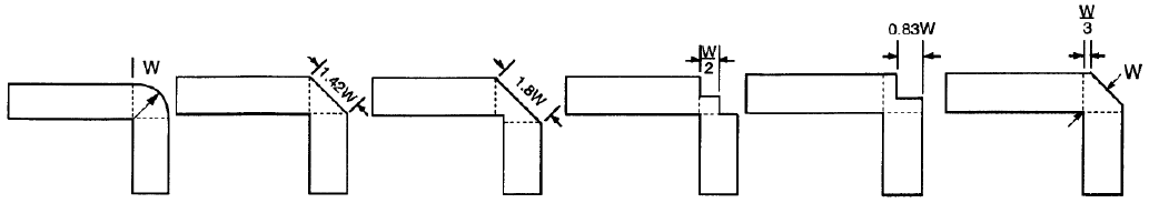
For our second board which we are having fabbed I made the microstrip way wider to correct for the ".062 board thickness. However I realized that I should have mitered the edge. So the third picture I have included shows the current design with a mitered edge.

Third image (current design):

I would like to know what you think of my design in general, and any tips/suggestions/corrections I should do to my microstrip and/or the rest of the design. I want the best range possible with this device. These boards as mentioned above will be on ".062 FR4 board with soldermask (two layer). Since this is a two layer design I have a double ground plane (top and bottom) with many vias across the whole board spaced at 0.1 inches.
Anyways I will include 3 pictures. The first one is the original. We had this board made on a mill machine. I designed the microstrip for using thin ".031 board, it is .055" wide which with that thickness of board should be around 50 ohms. However when we had it made at the school they used thicker ".062 board. However, it seems to be able to actually transmit a good distance. All shown dimensions are in mils (thousands of an inch)
For our second board which we are having fabbed I made the microstrip way wider to correct for the ".062 board thickness. However I realized that I should have mitered the edge. So the third picture I have included shows the current design with a mitered edge.
Third image (current design):
I would like to know what you think of my design in general, and any tips/suggestions/corrections I should do to my microstrip and/or the rest of the design. I want the best range possible with this device. These boards as mentioned above will be on ".062 FR4 board with soldermask (two layer). Since this is a two layer design I have a double ground plane (top and bottom) with many vias across the whole board spaced at 0.1 inches.