Continue to Site

Welcome to EDAboard.com

Welcome to our site! EDAboard.com is an international Electronics Discussion Forum focused on EDA software, circuits, schematics, books, theory, papers, asic, pld, 8051, DSP, Network, RF, Analog Design, PCB, Service Manuals... and a whole lot more! To participate you need to register. Registration is free. Click here to register now.

Weird transformer result in ads

Status
Not open for further replies.

An_RF_Newbie

Member level 3
Joined
Sep 1, 2020
Messages
64
Helped
0
Reputation
0
Reaction score
0
Trophy points
6
Activity points
507
Hello,
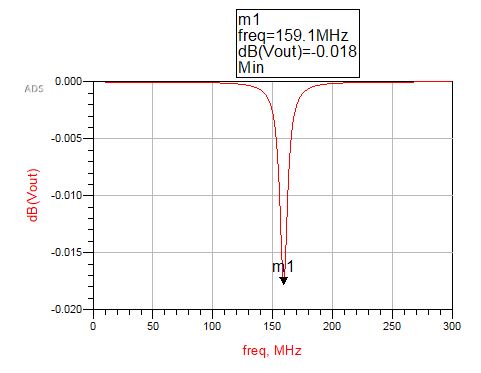
Here is my circuit before adding the transformer in ADS.
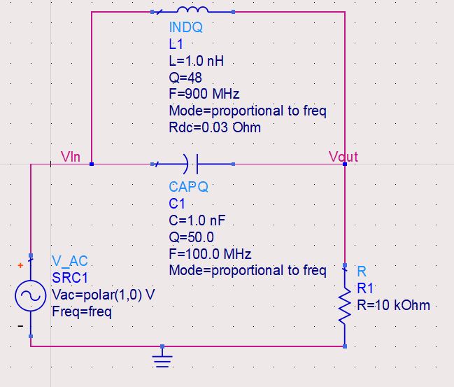
72.JPG


71.JPG


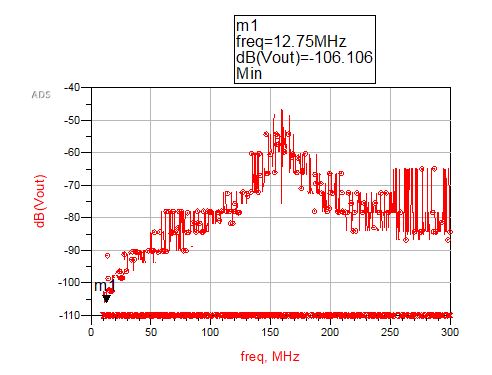
The resonance frequency response is acceptable. However, the result became weird after adding a transformer between the LC section and the source.
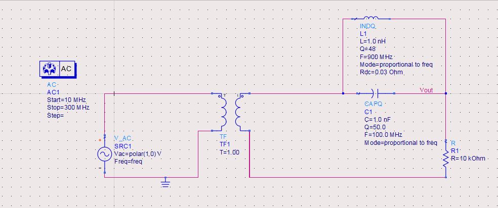
73.JPG

74.JPG

After changing the position of the Ground to LC section part, the result is acceptable again. But my problem is that I want to put transformers between LC sections, and I can't share ground between different stages, and the ground wire should be only at the end or near the source. How can I solve the ground connection in multistage transformer design?
 

Your technique works fine. Is there another way to put the different ground wires in ADS with different names?
 

I don't know what you mean by "different ground wires"? To measure voltage difference between two points I would simply calculate the difference in data display.
 

Thank you very much. As you can see in other software(such as Altium, ...), we can name ground with different names to isolate the various stages of the circuit. I need to know if it is possible in ADS as well.
 

Sorry, I don't understand what you are trying to do. To me, ground means one net, and there is nothing like "multiple isolated grounds". ADS had exactly one global ground. Anything else is another net.

Each net can have one name in ADS. If multiple nets are isolated, they can have different names.

It might be just an issue with wording, that you call multiple nets "ground" and I call them differently. For simulation any net can serve as a common return connection for multiple stages.
 
Thank you very much for your help.
I removed the transformer and added two resistors to my circuit (R2, and R3) the result is something weird as well. Could you let me know what my problem is?

62.JPG


63.JPG
 

Hi,

not that weird as you think.

See the diagram of post#7:
* focus on the numbers of the Y-Axis. They all are the same and all are very close to zero.

Simply that all numbers are the same shows that you are at the edge of the mathematical resolution of the system.
A graph going up and down ... with not changing values of the Y-axis is meaningless. It has the same meaning a straight horizontal line anywhere in the graphic. The ups and downs give no information at all.

Now all values are close to zero. Very close. You may see it as zero.
If you want to go into detail why it is not exactly zero:
--> it basically represents the amplification of the voltage divider R2/R1. The gain is 0.9999.... or -0.0008685dB

******
Now back to the graph at post#1:
Y-Axis numbers again show values close to zero. You could treat them as zero.
..or go into detail.
* It begins with a voltage divider of 0.03Ohms/10k (indeed not exactly zero).
* then there is the tiny influence of the resonance of L2 and C1. with a very low effect of just -0.018dB. Not really worth to mention.
* then it targets to true zero dB because of the idal "zero" series resistance of C1.

Conclusion:
Both graphs show almost the same: a rather straight horizontal line close to zero.

Klaus
 
I agree with Klaus. 1nH inductor at 300MHz has only ~2 Ohm reactance, so the output voltage across the 10kOhm load is almost the full source voltage. In dB() scale that is close to zero, as seen in your plot.
 
Status
Not open for further replies.

Part and Inventory Search

Welcome to EDABoard.com

Sponsor

Back
Top