Continue to Site

Welcome to EDAboard.com

Welcome to our site! EDAboard.com is an international Electronics Discussion Forum focused on EDA software, circuits, schematics, books, theory, papers, asic, pld, 8051, DSP, Network, RF, Analog Design, PCB, Service Manuals... and a whole lot more! To participate you need to register. Registration is free. Click here to register now.

weird behaviour from my amp circuite

Status
Not open for further replies.

Dummyeng

Member level 4
Joined
Mar 25, 2018
Messages
78
Helped
0
Reputation
0
Reaction score
0
Trophy points
6
Activity points
432
Hi
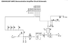
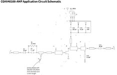
i used CGHV40100F https://www.wolfspeed.com/cghv40100-557

my design is almost the same as first one from datasheet but because i put sequencer and some other circuite in my design so i change a little it

my design is from 900 to 1300

first thing that i faced : when i put only inductor in power supply to gate my tr blow up !!!! and i should change tr and when i put only resistor (100ohm) it gets warm until it blow up and then my transistor blow up so i put first resistor and then inductor it gets better why did it happen?

second one in some frequency my power supply source in gate change its voltage and change it from 5 to 6 then 7 then 8 up to 9 and then goes back to 9 why happend it?


if you have any idea pls tell me

i change datasheet model for example amount of cap
gate power supply and other thing
 

Attachments

  • mydesign.jpg
    mydesign.jpg
    62.4 KB · Views: 119
Last edited:

1. When components burn it's pretty certain your circuit
draws overmuch current from the power supply.

2.
Your voltage varies because your circuit draws varying
amounts of current at different frequencies.
Your components create different impedance
(that is, inductive or capacitive impedance) at different
frequencies.

3.
The datasheet schematic has block diagrams which are empty
and un-labelled. Their function is unclear. Perhaps it's a
rough guide rather than a working schematic? And the
manufacturer assumes the customer is familiar with this
type of amplifier and details of its design? Does the manufacturer
publish design details in another data sheet?

4.
Question: Why do you apply power at a spot where the datasheet
schematic shows 0V ground? It puts the power supply near the top at
Vd. Vd presumably means V-Drain implying the transistor is N device.
 

what value is c16? is it 100 uf? (it probably should be if that is a power amp). try adding a 1 uf in parallel.

then the gate bias port....you have some words talking about a 4 turn inductor. well, that is probably not enough....are there shunt capacitors too? what value is the gate bias inductance...it might not be big enough.

try using current limited supply for the drain voltage to debug it that way if something is going wrong, you will not be wiping out the device.

how are you driving the gate? maybe you are forward biasing the junction and vaporizing it? try a current limiting resistor there.

and of course you have rf loads on the input and output, right?
 

thank for ur respond
if you allow me i will send two days later picture and ADS Schematic and lay out here for clarification

i changed it a lot(datasheet) i should send it
 

Adding a 1uF in parallel with C16 is a good idea, and I recommend adding also a 100nF in parallel, as Wolfspeed shows in the demo circuit.
Most probably your PA is oscillating at a low frequency.
 

Attachments

  • cghv.jpg
    cghv.jpg
    86.2 KB · Views: 95

Hi again

I consider sequencing for GAN

So it is my design

First of all I describe about real pic. Here you can see where I put gate voltage and that problem happen

I change my in three way

it should be almost 70nH and I think it was enough but when I put that inductor here my transistor explode it was very weird because I didn’t do rf on

I changed tr and put first inductor and resistor it got better but my output wasn’t enough and saw very weird behavior i describe them below

In some frequency my noise floor came up more than 20db and it happened from zero to I think to 2GHz

When I sweep between 1150 and 1165 my gate voltage that power supply showed me change from 5 to 9 (9 in 1157)

I put a capacitor parallel to inductor and after I don’t 1 or 2 minute my resistor explode and when I changed resistor my tr didn’t work and changed its gate impedance and as you know I burn it

As you know this kind of tr is expensive and I couldn’t do try and error


I know there are some fault that you can see in my design for example gate pin and other thing

Pls if you see them mention them but I don’t think this kind of problem because of them happen
--- Updated ---

4.
Question: Why do you apply power at a spot where the datasheet
schematic shows 0V ground? It puts the power supply near the top at
Vd. Vd presumably means V-Drain implying the transistor is N device.
i dont understand can u show me in datasheet
what value is c16? is it 100 uf? (it probably should be if that is a power amp). try adding a 1 uf in parallel.

then the gate bias port....you have some words talking about a 4 turn inductor. well, that is probably not enough....are there shunt capacitors too? what value is the gate bias inductance...it might not be big enough.

try using current limited supply for the drain voltage to debug it that way if something is going wrong, you will not be wiping out the device.

how are you driving the gate? maybe you are forward biasing the junction and vaporizing it? try a current limiting resistor there.

and of course you have rf loads on the input and output, right?
i put i think 500nf
i think inductor is enough as i explain above
ok thank
where should i put it and u explain more
yes i connect input to driver and output to load
Did you read "Connection Sequence for Power Amplifier" You have to read it..
yes i put sequencer and observe it
Adding a 1uF in parallel with C16 is a good idea, and I recommend adding also a 100nF in parallel, as Wolfspeed shows in the demo circuit.
Most probably your PA is oscillating at a low frequency.
ok i will put that
 

Attachments

  • eda.jpg
    eda.jpg
    879.1 KB · Views: 103
Last edited:

I wrote:
4.
Question: Why do you apply power at a spot where the datasheet
schematic shows 0V ground? It puts the power supply near the top at
Vd. Vd presumably means V-Drain implying the transistor is N device.

You wrote:
i dont understand can u show me in datasheet

Here is the schematic found on page 6. Where the power supply is, I added a label in green text. The voltage may not necessarily need to be 50V.

There are many ground icons. I believe J1 at left is where the signal is supposed to be applied.

CGHV40100F schematic.png
 

Status
Not open for further replies.

Part and Inventory Search

Welcome to EDABoard.com

Sponsor

Back
Top