Politecnico
Member level 1

- Joined
- Aug 28, 2013
- Messages
- 34
- Helped
- 1
- Reputation
- 2
- Reaction score
- 1
- Trophy points
- 8
- Activity points
- 316
Dear All
Hi,
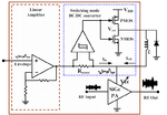
I am designing a Voltage Modulator to be employed in Envelope Tracking PA.

According to the circuit above, we have the detected envelope of the input RF signal as Vin to the voltage modulator. First, it goes through LINEAR AMPLIFIER stage and then HYSTERESIS COMPARATOR to drive / drive not the SWITCHING stage.
1) what is the least required GAIN and OUTPUT CURRENT of the Linear Amplifier Stage? Besides, Assuming input RF signal according to WiMAX or WCDMA standards, what is the envelope voltage range?
(right now, I have designed the linear stage with GAIN=55 dB. Is that enough or we need more?)
2) At the Comparator, What voltages does it compare? one side is the output of the Linear Amplifier, and what is on the other side?
3) Is TSMC 0.16um with bias of 3.3v suitable / sufficient to design the whole circuit?
Please correct me if any of my understandings about Voltage Modulator is wrong.
Since I am beginner in designing low frequency analog circuits, any comment is highly appreciated.
Hi,
I am designing a Voltage Modulator to be employed in Envelope Tracking PA.

According to the circuit above, we have the detected envelope of the input RF signal as Vin to the voltage modulator. First, it goes through LINEAR AMPLIFIER stage and then HYSTERESIS COMPARATOR to drive / drive not the SWITCHING stage.
1) what is the least required GAIN and OUTPUT CURRENT of the Linear Amplifier Stage? Besides, Assuming input RF signal according to WiMAX or WCDMA standards, what is the envelope voltage range?
(right now, I have designed the linear stage with GAIN=55 dB. Is that enough or we need more?)
2) At the Comparator, What voltages does it compare? one side is the output of the Linear Amplifier, and what is on the other side?
3) Is TSMC 0.16um with bias of 3.3v suitable / sufficient to design the whole circuit?
Please correct me if any of my understandings about Voltage Modulator is wrong.
Since I am beginner in designing low frequency analog circuits, any comment is highly appreciated.
