Continue to Site

Welcome to EDAboard.com

Welcome to our site! EDAboard.com is an international Electronics Discussion Forum focused on EDA software, circuits, schematics, books, theory, papers, asic, pld, 8051, DSP, Network, RF, Analog Design, PCB, Service Manuals... and a whole lot more! To participate you need to register. Registration is free. Click here to register now.

Vital glitches,many input changes

Status
Not open for further replies.

draser

Member level 2
Joined
Apr 1, 2016
Messages
47
Helped
0
Reputation
0
Reaction score
0
Trophy points
6
Activity points
421
Hello,

In my design i get some vital glitches and i think i know where do they come from.

Lets assume that i have a combinational circuit with INPUTS A,B,C and an OUTPUT E that depends from every input.These inputs are connected with flip flops but each flip flop is a part of a different component.

My problem is that the input A is changing i.e. at 0.01 ns ,the input B at 0.02 ns and the input C at 0.03 ns (each of them after the clock_rise_edge) . The problem is that each of them trigger the process and is changing the OUTPUT E but the output E cannot change so many times so fast and as a result i get a vital glitch.The final result is correct but does anyone know how can i avoid this vital glitch?


Can i make my design to check the input changes after i.e. 0.5ns so i can be sure that the output will change only once in every clock_period and not three times??

or are there any other solutions to fix this?

Thank you.
 

This sounds similar to a switch-bounce problem.
Or, perhaps your inputs A-B-C are causing a disallowed condition, which results in glitchy output at E?

Can you lengthen the pulses from A-B-C? So that the first arrival persists for a long enough time that any other arrival is irrelevant?

Your .01 nS timescale could be hard to work with.
 
  • Like
Reactions: draser

    draser

    Points: 2
    Helpful Answer Positive Rating
The problem is that each of them trigger the process and is changing the OUTPUT E but the output E cannot change so many times so fast and as a result i get a vital glitch.
This statement kind of confuses me. If you are doing a netlist simulation you shouldn't have any process statements that would exhibit this behavior...Is this a mixture of HDL and structural netlist VHDL?

VSIM has a -noglitch option that disables Vital glitches. I'm assuming this is a netlist simulation problem you are having and not some issue with HDL code where someone coded separate combonational process and FF process.

e.g.
Code:
signal sig1, sig2;
signal a_din;
signal a_qout;

comb_proc: process (all)
begin
  a_din <= sig1 and sig2;
end process;

sync_proc: process (clk)
begin
  if (rising_edge(clk)) then
    a_qout <= a_din;
  end if;
end process;

instead of coding it like this:
Code:
signal sig1, sig2;
signal a_qout;

process (clk)
begin
  if (rising_edge(clk)) then
    a_qout <= sig1 and sig2;
  end if;
end process;

This second code will behave exactly the same without having to enter the comb_proc process on every change of the RHS signals. Which will both improve the simulation speed and get rid of any "glitches" on the signals if there are any after delays inserted in the code for the sig1 and sig2 generation (another pet peeve of mine).
 
  • Like
Reactions: draser

    draser

    Points: 2
    Helpful Answer Positive Rating
This statement kind of confuses me. If you are doing a netlist simulation you shouldn't have any process statements that would exhibit this behavior...Is this a mixture of HDL and structural netlist VHDL?

VSIM has a -noglitch option that disables Vital glitches. I'm assuming this is a netlist simulation problem you are having and not some issue with HDL code where someone coded separate combonational process and FF process.

Yes thats right,my netlist simulation has the problem.
Well the problem is that i want to eliminate the vital glitches, because of them i cannot do a power estimation from the netilist.I get some out_of_range ramps/loads and i need to fix them or else my power estimation will not be accurate.If i use the -noglitch option , will vsim fix them or i will not just see the glitches?I attache the code of the component that has glitches at his adress+RW output ports.

If it helps in my check_design i get these warnings:
UCN-1 net is connecting multiple ports.
LINT-29 input port is connected directly to output port.
LINT-31 output port is connected directly to output port.

However none of the above nets/ports that i get these warnings has a vital glitch error.

+ report_design

Report : design
Design : interconnect
Version: G-2012.06-SP4
Date : Tue Apr 12 17:42:56 2016
****************************************

Design allows ideal nets on clock nets.

Library(s) Used:

fsd0a_a_generic_core_wc (File: /space/alexios/UMC_LIB/90nmSP/core/fsd0a_a_generic_core_wc.db)

Local Link Library:

{fsd0a_a_generic_core_wc.db}

Flip-Flop Types:

No flip-flop types specified.

Latch Types:

No latch types specified.

Operating Conditions:


Operating Condition Name : WCCOM
Library : fsd0a_a_generic_core_wc
Process : 1.00
Temperature : 125.00
Voltage : 0.90
Interconnect Model : worst_case_tree

Wire Loading Model:

Selected automatically from the total cell area.

Name : enG5K
Location : fsd0a_a_generic_core_wc
Resistance : 0
Capacitance : 0.0001382
Area : 0
Slope : 0.5
Fanout Length Points Average Cap Std Deviation
--------------------------------------------------------------
1 9.00
2 19.10
3 30.50
4 49.10
5 71.80
10 122.20
16 248.80
50 394.80
90 695.00


Wire Loading Model Mode: enclosed.

Timing Ranges:

No timing ranges specified.

Pin Input Delays:

None specified.

Pin Output Delays:

None specified.

Disabled Timing Arcs:

No arcs disabled.

Required Licenses:

None Required

Design Parameters:

None specified.

i must also refer that i test the netlist by connecting the inputs of netlsit with the outputs of 2 components, that are setting their outputs by reading data from a file every clock_period.
 

Attachments

  • fabric_component.txt
    1.5 KB · Views: 111

-noglitch option is supposed to be used for vital glitch removal. It's been years since I've worked on ASICs but I remember having that in my scripts when we used to run netlist simulations. I also remember a couple of other options but can't seem to recall what they were...ran vsim -help...
Code:
   -noglitch               Disable VITAL glitch generation
   +pulse_int_e/<percent>  Set interconnect pulse error limit as percentage
                           of delay
   +pulse_int_r/<percent>  Set interconnect pulse rejection limit as
                           percentage of delay
   +pulse_r/<percent>      Set path pulse rejection limit as percentage of
                           path delay

Beyond that I'm not going to be much more help, as I've been out of ASIC design for quite some time and don't know how the tool flow has changed. I'm assuming you run the simulation and need to get rid of the multiple transistions as they show up in the VCD file? If so the -noglitch is supposed to remove the vital glitch generation, but I'm not sure if it just hides the message or removes the glitches from the simulation.
 

nothing will be fixed my friend! just ignored temporarily.

So how am i going to find what is causing the glitch?You suggested me in a previous post 4 ways to fix them(set the maximum transition time,the maximum cap load,the transition time of the primary inputs of my circuit and the the load on all primary outputs of the circuit).If you use synopsys DC,could you give me an example with the commands i should use?Cause i do not know if i am setting them well..
The warning message only informs me:

Warning: VitalGlitch: GLITCH Detected on port O ; Preempted Future Value := 1 @ 150.158 ns; Newly Scheduled Value := 0 @ 150.211 ns;
# Time: 150143 ps Iteration: 1 Instance: ..../aw_1/U29

So i have no clue what does this mean and the fact that this is happening only in 3 of my 500 testing input values is really weird!

And why is this so important to fix them?I mean as far as the outputs of the design are correct and they have no glitches,why should someone bother to fix them?
 

And why is this so important to fix them?I mean as far as the outputs of the design are correct and they have no glitches,why should someone bother to fix them?

I can't really answer that, you indicated that they are causing a power analysis failure. Seems odd to me that 3 out of 500 test inputs would result in a failure to properly do power analysis...

- - - Updated - - -

Besides if you have a combinational circuit that has multiple inputs and the delays to the circuit are different for each input and the output is registered then there will be possible "glitches" on the output of that combinational circuit that will not pass the register as it's only capturing the final value. So I'm wondering if the glitches are real and you do need to do power analysis on them. I also don't get how one combination node out of the entire design is causing such a problem with the entire design, even it was occurring every clock cycle, I would think the rest of the design must be much much larger and would be the biggest contributor to the power usage.
 
  • Like
Reactions: draser

    draser

    Points: 2
    Helpful Answer Positive Rating
I can't really answer that, you indicated that they are causing a power analysis failure. Seems odd to me that 3 out of 500 test inputs would result in a failure to properly do power analysis...

- - - Updated - - -

Besides if you have a combinational circuit that has multiple inputs and the delays to the circuit are different for each input and the output is registered then there will be possible "glitches" on the output of that combinational circuit that will not pass the register as it's only capturing the final value. So I'm wondering if the glitches are real and you do need to do power analysis on them. I also don't get how one combination node out of the entire design is causing such a problem with the entire design, even it was occurring every clock cycle, I would think the rest of the design must be much much larger and would be the biggest contributor to the power usage.

Well cause of these glitches i have around 500 out_of_range ramps and 100 out_of_range loads.I dont know if the numbers have a real impact on my power analysis..How can i ascertain this?

When i write the vcd file of my testbench it captures all the values of every component,so it captures the glitches as well i guess.

Well this combinational component is part of my entire design.The registers of the rest design do not capture these glitches .Also these glitches should be a small portion of the entire power consumption,because i guess the registers consume the most power.
 

Well cause of these glitches i have around 500 out_of_range ramps and 100 out_of_range loads.I dont know if the numbers have a real impact on my power analysis..How can i ascertain this?
Maybe the solution is not in removing these glitches from the VCD file but telling the power tool to not do something else with those 500/100 problems. Maybe you should contact the FAE for the tool.
 

Lets say that my circuit has 3 inputs A,B,C and 1 output D.Each input is connected with a different output port AO,BO,CO.Is there any way to increase the propagation delay between the output BO to input B and between C0->C??

I need this in order to make sure that the data to B will arrive later from A and the data to C will arive later than B.This will help me satisfy the output delay of my circuit.
 

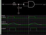
By inserting a series capacitor you generate a slight delay. Then a logic gate cleans up the signal. This is similar to the principle for making the proper sequence of timing signals (latch, reset, count enable) for my frequency counter as found in a Forrest Mims Engineer's Notebook.
 
  • Like
Reactions: draser

    draser

    Points: 2
    Helpful Answer Positive Rating
By inserting a series capacitor you generate a slight delay. Then a logic gate cleans up the signal. This is similar to the principle for making the proper sequence of timing signals (latch, reset, count enable) for my frequency counter as found in a Forrest Mims Engineer's Notebook.

Thank you,any idea how can i insert a series capacitor in vhdl?Is there a component like that?
 

This RC arrangement delays a pulse. Its function is known as an integrator.

RC integr delays pulse w AND gate follow.png

This not the same as the timing schematic I mentioned in post #12. Now as I look in the book, I see that some of the delay comes from NAND gates in series. (There are also series C, and some delay may come from the CR effect, however I could not make a simulation to portray the action as an effect by itself.)

A logic gate (or similar device) can be used to introduce a slight delay. The delay is tiny but that may be sufficient for your purpose. However I don't know whether VHDL models such behavior in that specific manner.
 

Now as I look in the book, I see that some of the delay comes from NAND gates in series. (There are also series C, and some delay may come from the CR effect, however I could not make a simulation to portray the action as an effect by itself.) A logic gate (or similar device) can be used to introduce a slight delay. The delay is tiny but that may be sufficient for your purpose. However I don't know whether VHDL models such behavior in that specific manner.

VHDL isn't designed to model analog behavior, so no the use of Analog techniques isn't going to fix the OPs problem. Adding more delay by editing the netlist (adding extra gates/buffers) will add delay to signals and merely spread the glitch out over a longer period of time. Perhaps that is the solution that the OP wants. But I still think this is a tool setup problem. As I don't know anything about the power analysis tool they are using, I haven't been able to comment beyond attempting to stop the simulator from producing a VCD file without the "glitches".

Ugly but might work...edit the VCD file to remove the glitches, you seem to indicate they only occur on a few specific nodes at multiple times, so I would think you could create a script to find the glitches and remove the extra transitions from the VCD file. I still think you should contact the FAE of the power analysis tool and find out what switches are available to disable the power analysis of "glitches".
 

Let me restate the problem:

The problem is that some of these glitches/violations cause some warnings when i try to measure the power consumption with synopsys PrimeTime.These warnings are:

i.e. 500 out_of_range ramps and 100 out_of_range loads.

I have read that these signals are caused by violations from my design,and that these warnings mean that PrimeTime will not count these signals on power analysis.I can have a power analysis but it will be not accurate.
However, PrimeTime has 2 modes: averaged and time-based.The second mode measures the power consumed by the glitches.

My question is,does the second mode measures also these out_of_range signals?is there a way to measure them without fixing the violations/glitches?
In order to remove them from the vcd file i need to know their value,is it 1X instead of 1 ,or sth like that?
 

Status
Not open for further replies.

Part and Inventory Search

Welcome to EDABoard.com

Sponsor

Back
Top