Continue to Site

Welcome to EDAboard.com

Welcome to our site! EDAboard.com is an international Electronics Discussion Forum focused on EDA software, circuits, schematics, books, theory, papers, asic, pld, 8051, DSP, Network, RF, Analog Design, PCB, Service Manuals... and a whole lot more! To participate you need to register. Registration is free. Click here to register now.

Vias in pads of 1812 ceramic capacitors?

Status
Not open for further replies.
T

treez

Guest
Hello,
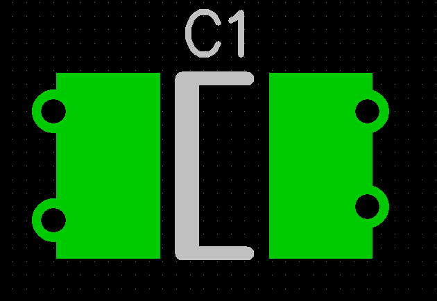
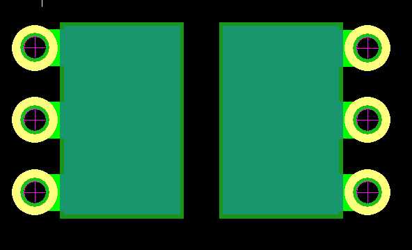
Is it acceptable to put vias in the pads of 1812 capacitors to get the current down to the bottom layer?....there is not enough room for enough vias outside of the pads as the board is so small.
 

Hi, to give you a complete answer you should specify the size of the via and the current you need to route.
As a general rule, vias in pads should be avoided. Indeed they can **** the solder paste during assembly, and this is especially true for "power" vias with large holes.
If you have room problems, you could move the vias on the outer border of the pads.
 
  • Like
Reactions: treez

    T

    Points: 2
    Helpful Answer Positive Rating
via 0.45mm ....the ripple in each cap would be about 300mA.....the current into the converter from the input Capacitor bank is 4 Amps average.
 

Hi,

If it is possible: avoid this.

You can use the place between the pads.under the capacitor. Use 3 or 4 smaller vias in parallel..

Klaus
 
  • Like
Reactions: treez

    T

    Points: 2
    Helpful Answer Positive Rating
via 0.45mm ....the ripple in each cap would be about 300mA.....the current into the converter from the input Capacitor bank is 4 Amps average.

The I suggest you to put two vias for each pad. You may put them like this:

 
  • Like
Reactions: treez

    T

    Points: 2
    Helpful Answer Positive Rating
The screenshot isn't clear because it doesn't show the solder mask. I suppose, the vias aren't separated from the pad by a soldermask feature. Related to the discussed problem of draining solder, the layout isn't essentially better than having the vias centered to the pad. Solder tends to wet continous copper areas in any case.

If vias in pad can't be avoided, I would use multiple small (0.25 to 0.3 mm drill) vias which are commonly used as thermal vias for ICs with exposed pad.
 
  • Like
Reactions: treez and kalbun

    kalbun

    Points: 2
    Helpful Answer Positive Rating
    T

    Points: 2
    Helpful Answer Positive Rating
The best way is to use filled vias, otherwise soldering problems could be encountered, even in the example above if the vias are not filled they will act as solder thieves and could starve the joint of solder.
 
  • Like
Reactions: treez and kalbun

    kalbun

    Points: 2
    Helpful Answer Positive Rating
    T

    Points: 2
    Helpful Answer Positive Rating
The best way is to use filled vias, otherwise soldering problems could be encountered

Agreed... but filled vias can be very expensive!!
Perhaps an intermediate solution could be to cover the via hole with solder mask, and to do so the suggested layout should work.
 
  • Like
Reactions: treez

    T

    Points: 2
    Helpful Answer Positive Rating
I agree that filled (plugged) vias are the best option, particularly copper plated plugs that can be used even in a BGA pad. It's my favourite option for boards with higher interconnect density.

Although it's no the primary focus of the original question, I see a strong relation to the design of thermal vias inside "exposed" IC ground pads.

It can be observed that unfilled thermal vias are becoming a standard technique in price sensitive PCBs. I see an interesting discussion of optimal design of unfilled thermal vias in the below linked Amkor application note: (Application Notes for Surface Mount Assembly of Amkor’s MicroLeadFrame(MLF) Packages) ,page 12f https://www.amkor.com/index.cfm?objectid=42EDA4C7-5056-AA0A-E2A372F025BF8729

They clearly show that an open via with tight solder mask opening on the bottom side is the best option (Of course only if plugging isn't available).

I'm using it since several years and didn't yet get any customer reports about assembly failure.

- - - Updated - - -

Perhaps an intermediate solution could be to cover the via hole with solder mask, and to do so the suggested layout should work.
PCB manufacturers usually insist on not being hold responsible for chemical residuals in tented vias that might endanger the boards's long term reliability.
 
  • Like
Reactions: treez

    T

    Points: 2
    Helpful Answer Positive Rating
Thanks, regarding the vias near the outside of the pad, -would you say its acceptable to have a 0.1mm clearance between the via's restring and the pad? (ie make the via as close to the pad as possible without actually touching it)......ie, presumably the solder would not be able to wick down the via because of the 0.1mm gap....or would you say relying on making such a small gap is not reliable?
 

Your PCB technology has a minimal soldermask feature size that shouldn't be undershot. 0.1 mm should be always O.K.

It's also possible (if you didn't already) to reduce the via's soldermask opening to a minimum, e.g. 0.3 mm drill, 0.4 mm soldermask pad.
 
  • Like
Reactions: treez

    T

    Points: 2
    Helpful Answer Positive Rating
thanks, sorry in my above, I meant the via is outside the pad by 0.1mm, but obviously as you know, there is the connecting track...and presumably you are declaring that a 0.1mm length of track to the via, which is covered in a 0.1mm "sliver" of solder resist, is enough to prevent wicking of solder down the via.?...presumably it is believed that if this 0.1mm length of track between pad and via was not covered in solder resist, then it would not be ok, and solder would wick from the pad, along the 0.1mm length 0f track, and end up wicking down the via?
 

I know what you mean. You're apparently assuming that the via soldermask has same size as copper (respectively copper plus standard oversize), but that's not necessary for vias.

A via can have a smaller soldermask opening as in the below screenshot, so the via can touch the SMD pad or even overlap it by a small amount and you still have soldermask separating the via hole from the pad.

 
Thanks FvM, I believe your above screenshot shows exactly what I need, thanks again.....I could presumably also make the solder resist entirely cover the via's annulus (or "restring" as its sometimes known)?...woops , you just explained that...yes, so basically I can overlap the via annulus slightly over the pad as long as the solder resist doesn't go on the soldering area.
...in any case, I believe you've solved the problem there........you also suggested possibility of 0.3mm vias in the pad itself (obviously with no solder resist on them), and I will keep this idea in reserve.
-thanks to all for ideas as they were all great though.
 

Status
Not open for further replies.

Part and Inventory Search

Welcome to EDABoard.com

Sponsor

Back
Top