cupoftea
Advanced Member level 5
Hi,
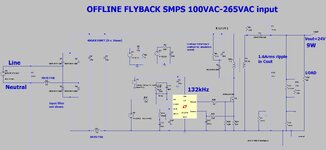
A competitor has an isolated Flyback SMPS as follows....
100-265VAC
132kHz
Vout = 24V.
9W
The attached is roughly what it is...(LTspice and jpeg)
As you can see, there is no common mode choke and no Y capacitors. However, the Neutral is poured throughout the PCB on an inner layer, and goes under most of the primary and secondary sides. This neutral copper pour , with the PCB substrate, acts as a decent Y capacitor to the rest of the circuit.
The two 1mH inductors could have been put in Line and Neutral so as to give some common mode inductance, but this wasn’t done, as you can see.
The isolation from primary to secondary is 1500VAC , and the creepage/clearance between pri and sec copper nets is down to 2.5mm , since the particular application, only needs this.(?)
Also, the SMPS is on a PCB some 3cm wide by 13cm long…..the AC input is on the left….then the X2 capacitor…..then next in the layout is the secondary side output caps….then the flyback transformer…then the RCD clamp and the primary DC Bus caps are on the “secondary” side….also the primary side filter caps are on the “secondary” side……(please don’t ask me why its higgledy piggledy like this…I don’t know)
Do you think we are being “stuffy” by refusing to accept this design from the place that did it for our competitor?
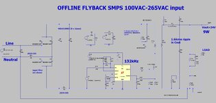