Continue to Site

Welcome to EDAboard.com

Welcome to our site! EDAboard.com is an international Electronics Discussion Forum focused on EDA software, circuits, schematics, books, theory, papers, asic, pld, 8051, DSP, Network, RF, Analog Design, PCB, Service Manuals... and a whole lot more! To participate you need to register. Registration is free. Click here to register now.

Vdc opamp feedback amplifier transfer function

Status
Not open for further replies.

yefj

Advanced Member level 4
Joined
Sep 12, 2019
Messages
1,180
Helped
1
Reputation
2
Reaction score
3
Trophy points
38
Activity points
7,111
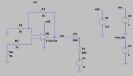
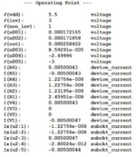
Hello,there is a circuit i saw which is supposed to amplify a DC signal input,in the circuit bellow its called Vdc as shown bellow.
I can see there is a feedback,In AC we have virtual ground and we do equation of currents.but here we have DC only input.
how do we calculate the Vout from Vdc and Va?
Thanks.

1620152010241.png
 

Hi,

"Virtual ground" is not for AC only. It's a function of a circuit. Mainly caused by an inverting Opamp circuit.
Your circuit is non inverting.

Every document or tutorial for "non inverting Opamp circuit" shows how to calculate gain and output voltage.
It's all standard.

Klaus
 

Hello Klauss ,If i undersatand you correctly given the circuit bellow.
V_plus=V_minus
also the current of V_minus/R1 is the current flowing on the R4 loop
(Va-Vout)/R6+(Va-Vout)/R5 flows into R4
so V_minus=[(Va-Vout)/R6+(Va-Vout)/R5]*R1
V_minus=V_plus (virtual ground)
I am stuck at this step.
where did i go wrong developing the expression for Vout?
Thanks.

1620159604652.png
 

The circuit has several useless components. R2 and R3 don't affect the output voltage, also R5 and R6 and the voltage at Va have no influence on Vout, at least if the output current capability of OPA495 isn't exceeded.
 

Your circuit essentially, as previous posters point out, reduces to this -

1620165199137.png


If your load on the output is infinity then eliminate R5paraR6 as no current flows
thru it if load R is infinite.

Note the common mode input range of this opamp does not include V+, worst case
it has to be, in your circuit, < Vdd - ~ .8V.

If you want circuit to work up to Vdd then OpAmp has to have RR input.

Note ignore the opamp part number shown. My slip up in simulator. But comments above
apply to yours.


Regards, Dana.
 

Attachments

  • 1620165497014.png
    1620165497014.png
    4 KB · Views: 110
Last edited:

The amplifier used in the original circuit is OPA495, its input voltage range includes the negative supply.
 

Hello Danadack ,So V_minus=Vplus=Vdc ?
how to start analizing your circuit
 

how to start analizing your circuit
This is a standard non inverting OPAMP circuit. Most basic. Thus it has been discussed maybe million times before.

V_DC --> V_plus
V_plus --> V_minus
V_minus --> V_R1
--> thus you can calculate I_R1
I_R2 = I_R1
--> thus you can calculate V_R2
--> thus you can calculate V_Out

Klaus
 

Hello Klauss, my OPAMP model is as shown bellow,LTspice is not allowing me to simulate its model so i used an alternative model just to simulate the principle,and see the transfer function in action.
I need to have this -3 Volts on the output side (its on the MAX 4231 original circuit) as shown bellow.
My circuit has two outputs
You said i should disregard R3 and R4 So V_plus=Vnon_inv=0.5v
So V_minus=0.5v also
so the current threw R1 is I_R1=0.5/R1 which is also the current that flows threw R2
0.5/R1=(Vout-0.5)/R2
Because R1=R2 Vout=1V which matches the simulation.
I=((1--3)/600)=1/150
Vout2=1-500*I=1-500*6.66*10^-3=-2.33V
which also matches to the simulation.
but in the the MAX4231 i also have the option of SHDN
So if i understand the data sheet bellow correctly when SHDN pin is 0V then the OPAMP output is GND and we have voltage divider between 0 and -3 instead of 1 and -3?
correct?

1620473513260.png


1620470365052.png

1620471941770.png
 

Attachments

  • 1620470082152.png
    1620470082152.png
    260.5 KB · Views: 100
  • 1620470318520.png
    1620470318520.png
    491 KB · Views: 101

Hi.

So if i understand the data sheet bellow correctly when SHDN pin is 0V then the OPAMP output is GND and we have voltage divider between 0 and -3 instead of 1 and -3?
correct?
Yes.

Klaus

added:
Usually there is the recommendation to drive the ouput only within the supply rails.
But you try to pull it below it´s supply rail.
Now it depends on how the output stage is designed.
In worst case it can´t handle negative currents referenced to GND.
A FET output should be able to drive the current both directions. Not sure how the OPAMP reacts on this reverse current.

Klaus
 
Last edited:
  • Like
Reactions: yefj

    yefj

    Points: 2
    Helpful Answer Positive Rating
when SHDN pin is 0V then the OPAMP output is GND and we have voltage divider between 0 and -3 instead of 1 and -3?
Not exactly. The output is disabled (high impedance). Negative output is limited to the forward voltage of substrate diode.
 

Hi,

Datasheet says "output is grounded with 10 Ohms", not high impedance.
Quite unusual, but it says so.

Klaus
 
Status
Not open for further replies.

Part and Inventory Search

Welcome to EDABoard.com

Sponsor

Back
Top