Continue to Site
Follow along with the video below to see how to install our site as a web app on your home screen.
Note: This feature may not be available in some browsers.
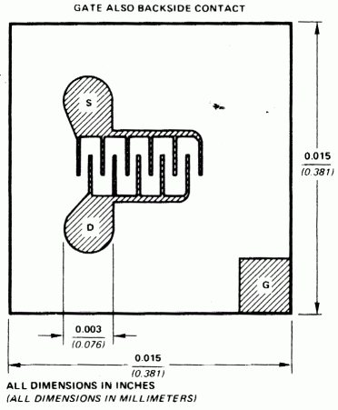
FvM said:J2 and J4 are almost operating in resistive region due to low Uds, but J3 is fully saturated. The circuit can be used as an amplifier anyway.
") hmmm.
hmmm.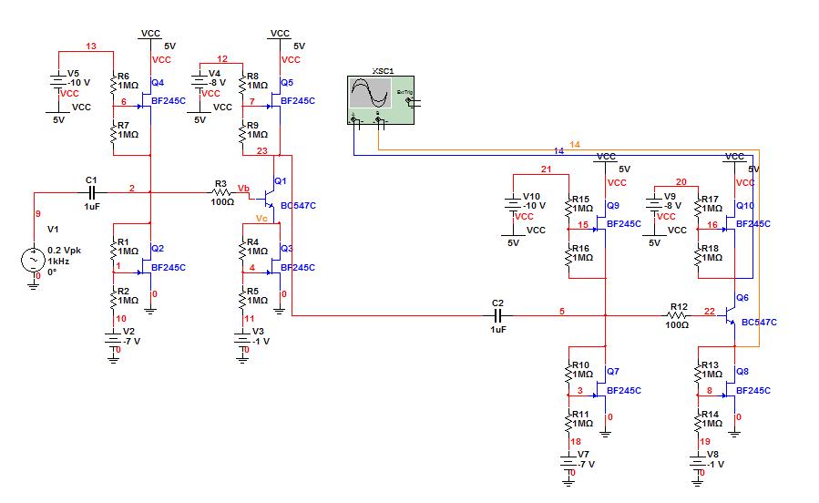
now i dont understand why in the output line signal is bad why is teh signal straight and not sine wave ?