cipi-cips
Member level 4
siliconix fet data book
I have a problem I need to build common emitter amplifire but instead of regular resistors that creates common emitter amplifer I need to put JFET as variable resistor
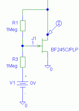
I think it is something like this but I am not sure, I tested this and it is not working lots of oscilation at output.
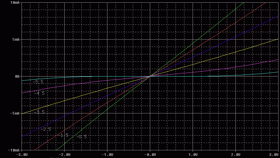
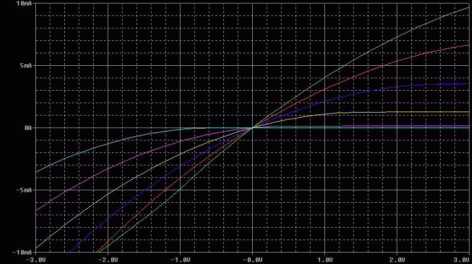
At the output there should be a signal that is amplified and there if you attach some voltage on the JFET (all 4) you should get variable amplifire
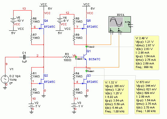
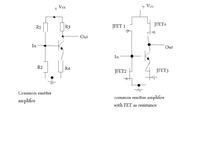
I have a problem I need to build common emitter amplifire but instead of regular resistors that creates common emitter amplifer I need to put JFET as variable resistor
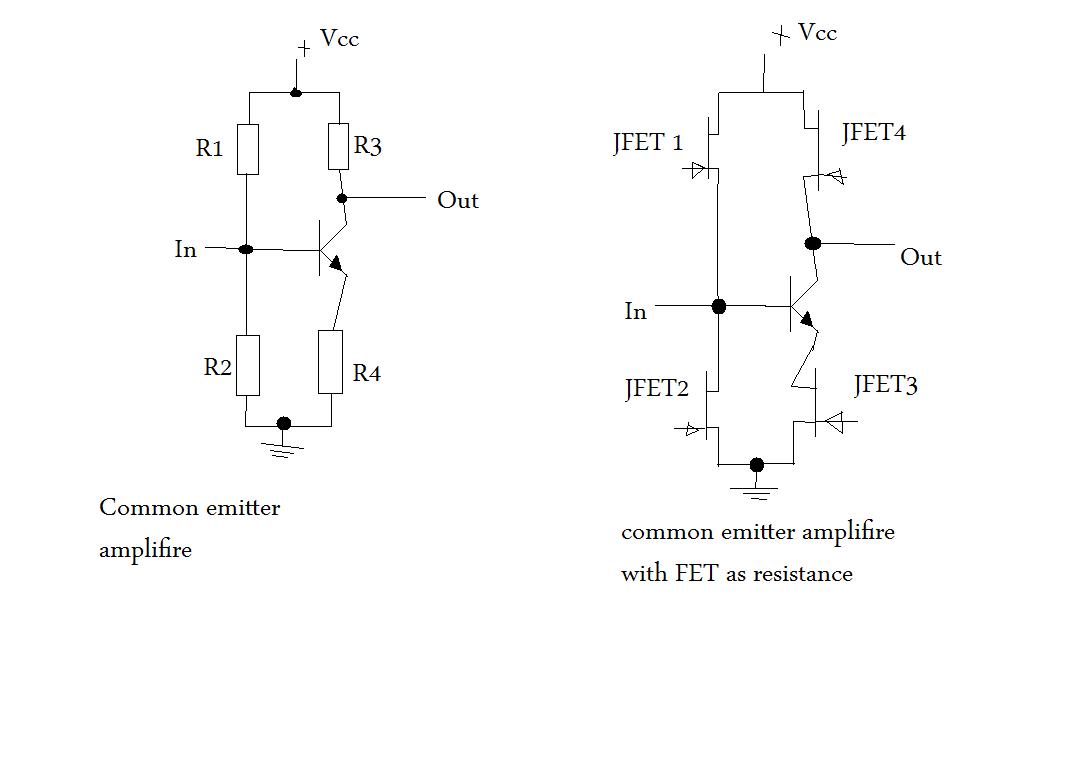
I think it is something like this but I am not sure, I tested this and it is not working lots of oscilation at output.
At the output there should be a signal that is amplified and there if you attach some voltage on the JFET (all 4) you should get variable amplifire
")