johnnyb7
Newbie level 3
Dear all,
I have two separate circuits which I want to connect using somewhat of a switch (most probably a BJT), which would either separate the two circuits or join them depending on whether the voltage on the first circuit is an active high (3.3 Volts) or an active low (0V).
ie. an active high should separate the two circuits (BJT in off) and an active low should join the two circuits (BJT in active).
I can not modify anything within the individual circuits, which is why I thought that this transistor should be placed in between the two circuits.

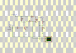
Attached you can find a Spice Layout of the two circuits and my idea of using a BJT. The first circuit (which can not be modified) is the scheme up to Resistor 'R1', the transistor Q2 was my idea to act as my switch, after Q2 comes the second circuit. The switch should switch depending on the values of V1 (either 3.3 or 0).
My idea was using an NPN and its emitter followed by the first circuit. In that case when active high is on V1, transistor Q1 is in active mode, which means less resistance to ground which ultimately means less base current, which should set Q1 in off. The vice-versa should happen when V1 is in active low. However, using this scheme I got a Vout of "2 and 0.6" instead of "roughly 3 and 0"
Does anyone have any ideas or could help me out with this problem. I may have also misunderstood the operation behind Q2.
I have two separate circuits which I want to connect using somewhat of a switch (most probably a BJT), which would either separate the two circuits or join them depending on whether the voltage on the first circuit is an active high (3.3 Volts) or an active low (0V).
ie. an active high should separate the two circuits (BJT in off) and an active low should join the two circuits (BJT in active).
I can not modify anything within the individual circuits, which is why I thought that this transistor should be placed in between the two circuits.
Attached you can find a Spice Layout of the two circuits and my idea of using a BJT. The first circuit (which can not be modified) is the scheme up to Resistor 'R1', the transistor Q2 was my idea to act as my switch, after Q2 comes the second circuit. The switch should switch depending on the values of V1 (either 3.3 or 0).
My idea was using an NPN and its emitter followed by the first circuit. In that case when active high is on V1, transistor Q1 is in active mode, which means less resistance to ground which ultimately means less base current, which should set Q1 in off. The vice-versa should happen when V1 is in active low. However, using this scheme I got a Vout of "2 and 0.6" instead of "roughly 3 and 0"
Does anyone have any ideas or could help me out with this problem. I may have also misunderstood the operation behind Q2.
")