Continue to Site

Welcome to EDAboard.com

Welcome to our site! EDAboard.com is an international Electronics Discussion Forum focused on EDA software, circuits, schematics, books, theory, papers, asic, pld, 8051, DSP, Network, RF, Analog Design, PCB, Service Manuals... and a whole lot more! To participate you need to register. Registration is free. Click here to register now.

use of ESD Diode[Medical_device]

Status
Not open for further replies.

zuirgham

Junior Member level 3
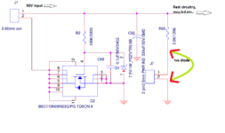
Joined
Mar 19, 2019
Messages
31
Helped
0
Reputation
0
Reaction score
1
Trophy points
8
Activity points
368
refer to fig1.
at j7 Connector, 12v LED(Part Number: 5110F1-12V) is connected. This LED is directly exposed to the outside world from the casing. when we do ESD testing at the LED spot,

case1: @ +-8KV, we are facing no issues.

case 2: @ +-15KV, the rest circuitry, mcu, lcd is going for a restart.

I was suspecting a voltage dip at the line, so i thought of using an ESD diode near to LED. I used this TVS diode (Part Number:SMBJ33CA) at the j7 Junction, and was still seeing the circuitry going for a reset, LCD was switching ON, oFF etc.

from a mechanical perspective, i was thinking of using an external glass casing atop LED, could there be any improvements in the circuit so as to withstand high KV ESD, or are there any more suggestions i can follow up before going for the next test
 

Attachments

  • fig1.PNG
    fig1.PNG
    50.7 KB · Views: 97

Hi,

A RESET is not necessarily a FAIL in ESD test. Some rules say the the device may temperarily go to an erroneous state but must to gain "controlled" state within a meaningful time. (often with the use of a watchdog)
Please check your ESD test rules.

Which ESD model do you use (MM, HBM, anything else...)

A schematic is only a part of the information needed.
We - or better say you - need to know where exactly the ESD current travles. An ESD probe has a GND connection and the HV tip. You need to be aware of the whole path between these two points. It´s stray inductance, voltage bounce on the path, traces nearby that become capacitively and/or magnetically coupled.

The ESD pulse is a high dV/dt pulse. What counts is rather trace impedance than trace resistance. This means you may use wide and thick traces with a resistance in the sub milliohms.. it does not matter. But the trace impedance may easily go to the hundreds of ohms. You need to think in HF not DC.

Rules: Keep the loop short. Keep the encolsed area small = signal the corresponding return_path need to be as cloase as possible. On a PCB this means: a GND_plane without cuts and other traces (in this area).

Klaus
I'm testing for IEC standard IEC 61000-4-2 Test Signal +15 kV , the LED was destroyed, and there was a reset occurred. Also, i'm using a panel mount LED, and it has long wires connecting to the board. Is There a way to protect the circuitry after injecting the ESD voltage ?
 

Hi,

To prevent a LED from overvoltage damage you should use some overvoltage suppression and negative voltage suppresssion.
Use a series resistor to limit the current and dissipate energy. It should not be a mechanically very small one ... to prevent an arc to jump over the whole resistor.
You should add a suitable overvoltage protection diode.
And you may add a fast parallel capacitor to slow down dv/dt.
All this should be close at the LED.

To prevent from accidental RESET we need to see the PCB layout and all the ESD current path.

Klaus
 

If the LED is "destroyed" can you determine the current
loop that would make it so? Was the event through the
encapsulation or a device lead (and if the lead, why is it
accessible to zapping?).

ESD is always about the current loop, even if the mechanism
is oxide rupture that's just because some portion of the
loop was allowed to develop a high voltage. Follow the
current around the circuit and you should be able to
determine likely branches for burnout or node-pairs for
overvoltage by "eyeballing" and knowledge of device
response to abnormal stress.

Reset behavior could relate to grounding schemes and
offsets imposed on one circuit block vs another (like a
POR circuit could be fooled if VDD is bumped down
below release-threshold by the ESD pulse). Ground
integrity, power integrity / interactions, signals that
have no choice but to follow a jacked ground branch
etc.
 

Status
Not open for further replies.

Similar threads

Part and Inventory Search

Welcome to EDABoard.com

Sponsor

Back
Top