Smillsey
Member level 5
Hi all!
I am laying out a project and using a USBC connector (as they are small) but only actually using USB2.0...
Anyway, my main question is how best to route the D+ and D- traces as the connector i am using makes it difficult to route D+ and D- to the 4 pins on the connector....
I am using this connector;
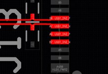
I have attached my current layout... only to two of the pins, i need to get those signals to the other two....
How should i approach this? I know USB2 wont need the same skew tolerances, but I want to ensure all signals are well skew matched and the overall length of the signals to the D+ and D- pairs are matched....
I am laying out a project and using a USBC connector (as they are small) but only actually using USB2.0...
Anyway, my main question is how best to route the D+ and D- traces as the connector i am using makes it difficult to route D+ and D- to the 4 pins on the connector....
I am using this connector;
I have attached my current layout... only to two of the pins, i need to get those signals to the other two....
How should i approach this? I know USB2 wont need the same skew tolerances, but I want to ensure all signals are well skew matched and the overall length of the signals to the D+ and D- pairs are matched....