Continue to Site

Welcome to EDAboard.com

Welcome to our site! EDAboard.com is an international Electronics Discussion Forum focused on EDA software, circuits, schematics, books, theory, papers, asic, pld, 8051, DSP, Network, RF, Analog Design, PCB, Service Manuals... and a whole lot more! To participate you need to register. Registration is free. Click here to register now.

Unknown diode need datasheet

Status
Not open for further replies.

boylesg

Advanced Member level 4
Joined
Jul 15, 2012
Messages
1,023
Helped
5
Reputation
10
Reaction score
6
Trophy points
1,318
Location
Epping, Victoria, Australia
Activity points
11,697
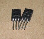
TO-220FP package - 3 leads with centre one common to both diodes.

EN210A 830GEN

No manufacturer logo

Can anyone point me in the direction of a datasheet?
 

check the attached fig and I think EN210A is pnp transistor. centre as base.
Ensure the transistor is out of circuit and take a digital Multimeter. Connect negative probe to base(centre pin of transistor) and positive probe to any one end of your transistor. Note the value.
And also, keep the negative probe in base itself, and shift the positive probe to other end of transistor. Note the reading.

The value which is higher is Emitter. And the value which is lower is Collector.

Hope this helps :) If im wrong, Please correct.
 

Attachments

  • EN210A_Transistors.jpg
    EN210A_Transistors.jpg
    83.3 KB · Views: 67

check the attached fig and I think EN210A is pnp transistor. centre as base.
Ensure the transistor is out of circuit and take a digital Multimeter. Connect negative probe to base(centre pin of transistor) and positive probe to any one end of your transistor. Note the value.
And also, keep the negative probe in base itself, and shift the positive probe to other end of transistor. Note the reading.

The value which is higher is Emitter. And the value which is lower is Collector.

Hope this helps :) If im wrong, Please correct.

Transistor? What's with the diode symbols then?
 

It's a PNP transistor. cathode is connected to each other.
 

I think what hemnath is tell you is that a PNP transistor has two PN junctions inside it just like the dual diode you show. From the outside it's difficult to tell a PNP transistor from a dual rectifier, it's only when you see the outside pins conducting to each other you can tell the difference.

Devices like those are mass produced with house codes for individual end users so you may never find a data sheet, especially after 30+ years since manufacture. It would be a fairly safe bet they are rated at around 50V and 5A and are probably fast switching types for SMPS.

Brian.

Hmmmmph....the confusing world of semiconductors.

I find it rather odd that the manufacturer would put diode symbols on a transistor when the same symbol is used for actual dual diodes. Well at least I am assuming that all the other components I have extracted, that have this same dual diode symbol, are indeed dual diodes.

They can't be that old because I extracted them from a dumped plasma or LCD TV earlier today.

- - - Updated - - -

I think what hemnath is tell you is that a PNP transistor has two PN junctions inside it just like the dual diode you show. From the outside it's difficult to tell a PNP transistor from a dual rectifier, it's only when you see the outside pins conducting to each other you can tell the difference.

Devices like those are mass produced with house codes for individual end users so you may never find a data sheet, especially after 30+ years since manufacture. It would be a fairly safe bet they are rated at around 50V and 5A and are probably fast switching types for SMPS.

Brian.

Hmmmmph....the confusing world of semiconductors.

I find it rather odd that the manufacturer would put diode symbols on a transistor when the same symbol is used for actual dual diodes. Well at least I am assuming that all the other components I have extracted, that have this same dual diode symbol, are indeed dual diodes.

They can't be that old because I extracted them from a dumped plasma or LCD TV earlier today.

I find it hard to drive past a dumped tv these days lest I miss some buried semiconductor treasure :)

I have used a few salvaged components now - tv power transistor for a high current voltage regulator circuit, a rectifier schkotty diode from a PC power supply and the neon bulb that I have used for my tesla antenna circuit also came froma TV circuit board.

I have quite a collection of stuff now. Heaps of metal oxide and wire wound resistors, a few dozen tv power transistors, a couple of dozen small mosfets ranging from 60V to 800V, opamps, comparators, a couple of full amplifier ICs, lots of LEDs.

Re-use and recycle and all that.
 
Last edited:

I find it rather odd that the manufacturer would put diode symbols on a transistor when the same symbol is used for actual dual diodes.
If there are diode symbols marked on it then it probably is a dual diode, as you guessed.

You didn't mention those markings in your description in post one - hence the confusion.
 

I think what hemnath is tell you is that a PNP transistor has two PN junctions inside it just like the dual diode you show. From the outside it's difficult to tell a PNP transistor from a dual rectifier, it's only when you see the outside pins conducting to each other you can tell the difference.

Devices like those are mass produced with house codes for individual end users so you may never find a data sheet, especially after 30+ years since manufacture. It would be a fairly safe bet they are rated at around 50V and 5A and are probably fast switching types for SMPS.

Brian.

i think it is impossible to tell difference between 2x diodes and pnp bjt with just a multimeter. they would both give same results no ?
but a bjt checker might be used to see if its actually a bjt, or just 2 diodes connected.

it is very strange to have symbols like that on the package, but who can tell with china manufacturers ?
 

i think it is impossible to tell difference between 2x diodes and pnp bjt with just a multimeter. they would both give same results no ?
Many multimeters include the ability to measure transistor hFE. A dual diode should give an abnormal reading with that test, probably about zero or one
 

Many multimeters include the ability to measure transistor hFE. A dual diode should give an abnormal reading with that test, probably about zero or one

yes of course. that is what i meant by bjt checker
 

excellent work !! how did you find that ? i looked and looked....

I have found that the first few letters of the part name, that are often ommitted, make all the difference. The problem is you have to know what they are.

For example when I first started doing this, it used to take a great deal of searching to find a datasheet for a K2934. You often come up with dozens and dozens of obviously irrelevant semiconductors.

But as soon as you search for 2SK2934 you usually come up with the data sheet in the first google page. Knowing to add the SK is the key.

So presumably adding the FM made the difference here.

Thanks for that guys any how - I have now added 5 rather useful schottky diodes to my collection if salvaged semiconductors.
 

Easy, I went to the web site wizpic linked to, it shows thw original picture and states that Sanken make them.
Then I went to Sanken's web site and searched for 210A, it comes up with the data sheet as the first item.

Brian.
 

The case also clarifies that you shouldn't trust second hand information like that saying it's a transistor.

Checking the device with a multimeter would have easily revealed a schottky diode, by the way.
 

Checking the device with a multimeter would have easily revealed a schottky diode, by the way.

excellent point. unfortunately we didn't know we were looking at a schottky device when we started, but a meter reading would have given a strong clue.
 

Even though the OP's problem is solved, the following can help others in the future in determining whether a 3-pin device is a transistor or a double-diode. You will need an analog multimeter for this. Also note that, in ohmmeter mode, most analog MMs usually put out a +ve voltage on the BLACK probe and -ve on the RED probe.

A double diode will have about the same reverse breakdown voltage for each diode whereas, with a junction transistor, the b-e junction has a lower breakdown voltage (usually around 5-6V) than the b-c junction. Here's how to find out which is which.

Set the analog MM to a high resistance range (x10k or x100k). In most analog MMs, this range uses an internal 9V battery whereas the lower resistance ranges use a lower voltage - 1.5 or 3V. Now, 9V is high enough to cause reverse breakdown in the b-e junction but not in the b-c junction. If you place the probes to the junctions in the reverse direction, the b-c junction will show only a tiny leakage current, but the b-e junction will breakdown and show a much lower resistance.

Note: Repeatedly causing reverse breakdown in the b-e junction for long periods can degrade transistor current gain. But this effect is negligible for brief measurements.
 

Status
Not open for further replies.

Part and Inventory Search

Welcome to EDABoard.com

Sponsor

Back
Top