Continue to Site

Welcome to EDAboard.com

Welcome to our site! EDAboard.com is an international Electronics Discussion Forum focused on EDA software, circuits, schematics, books, theory, papers, asic, pld, 8051, DSP, Network, RF, Analog Design, PCB, Service Manuals... and a whole lot more! To participate you need to register. Registration is free. Click here to register now.

Understanding feedback requirement of a switcher IC

Status
Not open for further replies.

mrinalmani

Advanced Member level 1
Joined
Oct 7, 2011
Messages
463
Helped
60
Reputation
121
Reaction score
58
Trophy points
1,318
Location
Delhi, India
Activity points
5,285
Hi!
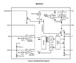
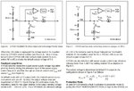
I am using NCP4371 which is a flyback converter switcher IC that uses a optocoupler for feedback.
I need to use this IC for buck topology. The error in output voltage and current is indicated at the DRIVE pin of the IC.
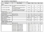
The specification for voltage and current OTA is also mentioned. (Please refer to the images)
My doubts are:
(1) OTA gain is specified to be 1. Does this mean that the OTA will sink 1A current if the error (V_out - V_ref) = 1V? This is a large amount of current!
(2) Says minimum OTA sink current = 2mA. What can this possibly mean? Does this mean that this is the quiescent current at zero error?

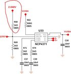
Please help me decide an appropriate resistor value that when connected to the DRIVE pin will give a meaningful error value that can be fed to the ADC of a microcontroller.
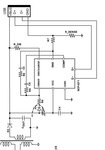
(I have also attached my schematic... is this OK?)

Thank you
 

Attachments

  • Capture10.JPG
    Capture10.JPG
    44.9 KB · Views: 86
  • Capture11.JPG
    Capture11.JPG
    70.3 KB · Views: 90
  • Capture12.JPG
    Capture12.JPG
    132.9 KB · Views: 87
  • Capture13.JPG
    Capture13.JPG
    31.5 KB · Views: 94

Small signal gain of the OTA is not going to extend
indefinitely. There will be a max output current. For
design purposes however you need to stay below the
minimum you list from the spec (this is the minimum
of the maximum current, like, given some input error
voltage condition).

A=1, you should scale to more reasonable terms.
Like 1mA/mV. So +2mV error would put you at
2mA. But you want to be able to deal with both
negative and positive error, so you want a load
that pulls -1mA at the balance point. Then +1mV
error makes 1mA, -1mV makes -1mA at the EA
output.

The ADC/uC path, I'd use a separate instrumentation
amplifier that makes its own gain (like maybe A=1000)
to gain up and center (in the ADC input span) the
error signal. Or perhaps even an independent
isolator with a different gain factor, which would
give you less meddling with the converter feedback
and an independent look at the supply voltage.

What works for the error amp, with its downstream
gain, is not what you want for monitoring. Unless
dirt cheap is the word. And even then you are going
to buy some sort of part.

You might consider that switch duty cycle is a fair
proxy for error amp input error voltage (other things
are in it, though, like VIN/Vout_set ratio) and look
at that (maybe integrated to a low voltage ~DC
value) for crude sanity monitoring. If you want an
accurate output reading then I'd go with the independent
sense path and a selected gain / offset to make the
ADC happy (inclusive of some fault / overrange margin
where you might still want monitoring fidelity).
 
Thanks for the reply!
My concern here is that the maximum guaranteed sink capability of the OTA is 2mA and since it has a gain of 1, just 2mV of error will sweep the full range of the available current limit. 2mV is small enough to be ignored but however here we are getting a full swing in just 2mV difference.
Am I getting this wrong? Is the gain suppose to mean 1mA/V?
Confused what to do...
 

You didn't yet notice that both control amplifiers, voltage control amp with input COMP and current limiting with input ISNS have an external RC circuit setting the PI controller gain. The said 2 mV are an amplifier input voltage but not the related error signal. Analyze the circuit as control system and you'll understand how it works.
Is the gain suppose to mean 1mA/V?
Surely not. It's S, A/V or mA/mV.
 
Thank you for the reply...
It makes sense now that the 2mV is the amplifier input signal and not the absolute error.
However, I'll have to admit that at this point I am totally out of touch with control systems and it would take me a few days before I can start analyzing circuits from a control-system point of view.
I can do that surely for future designs but for the current project, I have already exceeded the deadline.
Is there a quick reference that can help me decide the external compensating network resistor value?
Also, I have come across another switcher IC CHY103 by "Power Integrations".
This IC directly manipulates the feedback voltage by the help of internal band-gap.
I have attached a clipping of the datasheet page. Is this IC a quicker and better solution?
The aim is to send output error signal to a micro controller that is controlling the power converter.
 

Attachments

  • Capture14.JPG
    Capture14.JPG
    159.6 KB · Views: 84

Status
Not open for further replies.

Similar threads

Part and Inventory Search

Welcome to EDABoard.com

Sponsor

Back
Top