Continue to Site

Welcome to EDAboard.com

Welcome to our site! EDAboard.com is an international Electronics Discussion Forum focused on EDA software, circuits, schematics, books, theory, papers, asic, pld, 8051, DSP, Network, RF, Analog Design, PCB, Service Manuals... and a whole lot more! To participate you need to register. Registration is free. Click here to register now.

[SOLVED] ULN2803 and PWM problem

Status
Not open for further replies.

neillsun

Junior Member level 2
Joined
Jul 12, 2007
Messages
20
Helped
0
Reputation
0
Reaction score
0
Trophy points
1,281
Location
London, UK
Activity points
1,442
I am busy building the following: https://www.instructables.com/id/A-sunrise-and-sunset-lamp-with-LEDs/?ALLSTEPS.

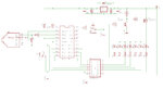
I appear to have a problem driving the ULN2803A with the PWM controlled FET (IRF520)... or with the ULN2803A being driven by a PWM controlled FET...

I currently have 7 LEDs wired to the ULN2803 outputs, resistors wired to ULN output and cathodes soldered together and connected to the +20V.

The symptoms are: the LEDs that should be on light up at full brightness and don't get dimmer with each decrease in the PWM duty cycle, and the LEDs that should remain OFF slowly get brighter with each decrease in the PWM duty cycle.

If I remove the PICAXE pwmout and pwmduty commands, and set pin B.3 high (to switch the FET on) the LEDS that should be on are on, and the LEDs that should be off are off.

As far as I can tell the problem does not lie with the stripboard design, and neither does it lie with the PICAXE.

I'm wondering if the ULN2803 has a problem with its GND pin being controlled by a FET, whose gate is PWM controlled. I can think of no other reason why I get the ULN switching output pins that should remain off.

I have tried swapping the FET with an NPN transistor, swapping the ULN2803A for another, with the same results each time.

My next step will be to solder up an array of NPN transistors to replace the ULN2803...

Does anyone have any thoughts?

Thanks,
N.
 

That isn't the cleverest of designs, when the FET is off there is risk of damage to the MCU and the ULN2803.

However, your problem is almost certainly that there is insufficient gate voltage to make the FET conduct properly. The data sheet states 250uA drain current at 4V drive in worst case conditions. You might get better results with a transistor array but the real solution is to use logic gates in the Picaxe outputs so the PWM drive to each LED is always VSS to VDD then add the current amplifiers afterwards.

Personally, I would do all the PWM in software but I'm not sure if the Picaxe allows you to do that. (hint: use the PWM to change the pins fom inputs to output mode)

Brian.
 
Thanks Brian.

For the sake of experimentation - and to quell my own curiosity - I think I'll try the transistor array either way.

I realise I wasn't particularly clear with my PWM explanation - this is handled by the PICAXE on pin B.3, with the remaining 7 PortB pins as outputs for the LEDs. The PICAXE has a built-in PWM handler that runs independently of the main timer.

I don't understand your suggestion of using the logic gates in the Picaxe outputs so the PWM drive to each LED is always VSS to VDD then adding the current amplifiers afterwards. - do you mean use PWM on each output pin of the PICAXE to drive the ULN input pin rather than switching the entire ULN? This would make sense to me, but I don't think the PICAXE can handle this.

Thanks for you input!!

N.
 

That's exactly what I meant. I've never dealt with a Picaxe so forgive my ignorance over the PWM output. I see two problems at the moment:

1. the ULN2803 has input series resistors and darlington outputs so it needs a relatively high voltage to make it fully conduct, combined with it's ground being lifted slightly by the FET it may not be possible to make it saturate.

2. When the FET is turned off, the entire ULN2803 and LED loads are connected between the Picaxe outputs and +24V, effectively their ground becomes disconnected. This could damage the Picaxe outputs and also reverse bias the ULN2803 internal transistors to the point where they are damaged too.

Regarding point 1, you should be able to use single transistor driver stages as the current is relatively low. I suspect the original designer did this (as in their photograph) and they never tried it with a ULN2803. For point 2, controlling brightness by disconnectig the ground will not stop the potential for damaging the devices, it would be better to adapt the circuit so the PWM fed the base of a small bipolar transistor and that in turn controlled a switch in the 24V line feeding the LEDs. In other words, use high side switching instead of low side.

Brian.
 
I doubt that the "genious" PWM circuit has been ever used as shown.

As clarified in the datasheet, ULN2803 has substrate diodes at in- and outputs, so the ground pin will be hold low by the input pins driven to 0V. In addition parasitic substrate transistors will be turned on and feed the outputs in off-state.
 
Thank you both.

I'll give the transistor array and switching high side a try. I'll let you know how it turns out.

N.
 

I'm waiting for the logic level P-channel MOSFET I ordered to handle the high side switching. I'm planning on adding a 100K/1M (?) pull-down resistor to the gate to stop it floating. I'll leave the ULN in place for now. no point in building an array if I don't need to.
 

I'm missing something, aren't I??

I've connected the p-Channel MOSFET (FQP27P06) as follows: Pin 1 (Gate) connected to MCU pin B.3 (PWM pin) with 1M pull-down resistor. Pin 2 (Drain) connected to LED cathodes and Pin 3 (Source) connected to +24V.

The LEDs turn on at full brightness, no matter what I do with the Gate. I can ground it, connect to +5V, use pull-up resistor. disconnect completely! The LEDs stay on at full brightness.

I don't have a 'scope or logic analyzer, but putting a voltmeter on the PWM pin I can see the effective voltage change with as the duty cycle changes.

Bit out of my depth here apparently! Any help?

Thanks,
N.
 

Show us a schematic please.

To turn the MOSFET off you have to raise the gate voltage to the same as the source voltage and it sounds like you are expecting the Picaxe to raise the PWM voltage to 24V. Use a second transistor, a small signal NPN type should do. Ground the emitter, connect the PWM to the base through a suitable resistor (2.2K if there isn't one in the Picaxe) and connect the collector through 47K to the 24V line. The collector should go from 24V to almost zero as the transistor switches on and off. Now connect the collector to the gate of the MOSFET through another resistor so the gate sees the full 24V swing.

Brian.
 

Hi Brian,

Thanks, I had thought of a second transistor, but didn't think it necessary as the FET I am using is a logic level, so only requires 5V at the gate.

Maybe I have something else wrong, but I am not seeing it.

N.
 

I think so too :)

A MOSFET, at least the common enhancement mode types like you are using, works like a voltage controlled switch. The voltage between the source and gate decides whether the switch between the source and drain is open or closed. When no voltage is present the switch is opened and no current can flow though it, when the voltage is high enough (logic level voltage in your case) the switch is closed and appears almost as though there is a wire link across the source and drain.

In your circuit, the brightness is controlled by the PWM signal. Although you measure it changing on a test meter (because it tends to average the readings) it is actually always going from 0V to VDD. The PWM signal is at constant frequency but within each cycle the amount of low and high period is being varied. The apparent brightness change in your LEDs isn't because the amount of current through them is being changed, it's because the amount of time they are lit and unlit is varied but so fast that your eyes can't perceive the flickering.

With the high side MOSFET connection you have at the moment, it will be conducting 100% of the PWM cycle because the output pin of the Picaxe can only go between 0V (the part of the PWM cycle that is low) and 5V (the PWM high part). As it is connected to the MOSFET gate and it's source is at 24V, the voltage across the source and gate will change from (24V-5V) 19V when the Picaxe pin in is high and 24V when it is low, both making it fully conductive (switched on). To make it turn off, the source to gate voltage must be zero so the PWM high level has to be shifted up to 24V so the gate and source are at the same voltage.

That's where the second transistor comes in. The Picaxe PWM output is relative to it's ground pin so you want that to be able to turn a higher voltage switch on and off to control the MOSFET. If you connect a bipolar NPN transistor as I suggested, emitter to ground and base to the PWM through a resistor, it will also act like a switch, this time from collector to emitter (ground) or isolated. The transistor will not have the 5V restriction of the Picaxe output so it can be connected to a higher voltage, in this case the 24V through the collector load resistor (the pull-up resistor to 24V). The collector voltage will swing from 24V to 0V which is exactly what you want to drive the MOSFET.

Brian.
 

I'll have another bash at it this evening and will submit a schematic.

Thank you for the help so far!

N.
 

Hi Brian,

Thanks for the explanation. I think I am getting my head around it now.

I have added the transistor to the schematic - if you wouldn't mind casting your eye over it.

Thanks,
Neill.
 

Attachments

  • 7-Strip Sunset Lamp_FET.jpg
    7-Strip Sunset Lamp_FET.jpg
    214.4 KB · Views: 127

Looks good to me.

My only comment would be that if the Picaxe doesn't have an internal pull-up resistor on P$19, I would connect R12 from it's pin to +5V so it goes to 5V when the switch is open and ground when its closed. Otherwise when the switch is open the pin has nothing driving it and might do wierd things. You can safely increase R12 and R10 to a higher value as the current through them is negligible, 47K should be fine and it will decrease the overall current drawn by a few mA.

Brian.
 
Thank you very much.

I will try this tomorrow. (I didn't add the pull up to P$19 on this schematic, but I did add it to my (hand drawn) stripboard layout.

N.
 

SUCCESS!! Ha!

Thanks Brian. I reduced the value of the 47k pullup resistor (NPN collector to +24V) to 520R ... the 47k didn't allow the voltage to FET Gate to be high enough to switch the FET off. (Sound like I know what I'm talking about, huh??)

Anyway, my test circuit works now. Thank you very much indeed.

Neill.
 

Status
Not open for further replies.

Part and Inventory Search

Welcome to EDABoard.com

Sponsor

Back
Top