Continue to Site

Welcome to EDAboard.com

Welcome to our site! EDAboard.com is an international Electronics Discussion Forum focused on EDA software, circuits, schematics, books, theory, papers, asic, pld, 8051, DSP, Network, RF, Analog Design, PCB, Service Manuals... and a whole lot more! To participate you need to register. Registration is free. Click here to register now.

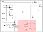
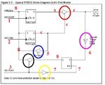
Typical PORTD Block Diagram (in I/O Port Mode OF 16F877A MCU

Status
Not open for further replies.

PA3040

Advanced Member level 3
Joined
Aug 1, 2011
Messages
883
Helped
43
Reputation
88
Reaction score
43
Trophy points
1,308
Activity points
6,936
Dear All,
Please see the attached picture for me

This is the understanding purpose of all parts of the PORTD block diagram

I would like to understand step by step than all together at once

Therefore the attached picture have two D flip flop ,both are smiler to each other, Am I correct?

The D flip-flop tracks the input, making transitions with match those of the input D. The D stands for "data"; this flip-flop stores the value that is on the data line. It can be thought of as a basic memory cell

Let say I want to configure PortD pin 0 as an out put
Then
first bannksel
BCF TRISD,0

It would be much appreciated if some one can teach me the data flow using attached picture

Thanks in advance
abc.jpg
 
Last edited:

Dear 2k12,

Thanks for advice
 

Dear 2k12,

Thanks for advice

Hi,

As in the datasheet, you normally Clear the Data buffer before changing the Tris register to ensure the port pin is low.

As you say the 3 flip flops interact with each other to control the flow of the Data Bus by means of the 4 control signals RD and WD Tris and Port.

The one inverter and 3 tri state buffers are used to create the correct logic level to control the flip flops.
Yellow being a simple inverter, Blue and black being simple tri state buffers so when a control signal is applied the data flows through, but when the control signal is off the output goes hi impedance / invisable.
Red is the same but the control pin needs a logic low to activate.
The purple Schmitt trigger ensures a clear distinction between a high and low input signal.
 
  • Like
Reactions: PA3040

    PA3040

    Points: 2
    Helpful Answer Positive Rating
Hi wp100,
Thanks for the reply
Let's we think of BCF TRISD,0 Instruction

I need to know this instruction effect to the (WR TRIS) which is clock bit of the middle flip flop or Data pin of the same FF

Please advice
 
Last edited:

Dear All,
Let's we suppose BCF TRISD.0 Instruction. by which set the PORTD bit 0 as an output. In this case Location "C" in above picture must set to 1 then Z=X by which PORTD bit 0 configure as an output

Question 1. In the above picture the D flip-flop is working at high to low transition. Am I correct?

Question 2. To set C to 1( see picture ) the tris latch data bit must set to 1 and WR TRIS must goes to low

BCF TRISD,0 command send the low to clock bit Am I correct.
Please more advice is deeded
Thanks in advance
 

Hello,

As in the actual datasheet, a person typically Clear the Information buffer before changing the actual Tris sign up to guarantee the port pin number is actually reduced.

When you repeat the three flip flops communicate with one another to manage the circulation of the Data Bus by way of the 4 handle signals RD and also WD Tris as well as Port.

Usually the one inverter and 3 three express buffers are employed to create the correct logic degree to manage the particular shoes.
Yellow being a simple inverter, Glowing blue and black being straightforward three condition buffers when a manage signal is used the info moves via, however when the control sign is actually from the end result will go hi impedance Or invisible.
Red-colored is the same however the control pin number needs a logic reduced to activate.
The pink Schmidt result in guarantees a definite distinction between a higher and also reduced feedback sign.
 
  • Like
Reactions: PA3040

    PA3040

    Points: 2
    Helpful Answer Positive Rating
Dera respons,
Thanks for the reply,
Actually I need to know is, what is the logic behavior when configure PORTD bit 0 as an out put

Command is BCF TRISD,0

finally I know C (in picture) should logic one (1).
What are the logic level of other locations, that should effect when executing the above command

Please advice
 

.... set the PORTD bit 0 as an output. In this case Location "C" in above picture must set to 0 (low) then Z=X by which PORTD bit 0 configure as an output
...
As wp100 and response01 wrote the red colored buffer's enable level on "C" is low, NOT high (see its small circle :) )
 
  • Like
Reactions: PA3040

    PA3040

    Points: 2
    Helpful Answer Positive Rating
Dear zuisti,
Really thanks for the reply,
I got the point from your single sentence explanation and understood the way it explained by wp100 and response01.

If c is 0 then Q OF tris latch should be 0. if Q =0 then at the same time D should be 0 of tris latch (see the picture above my first post )

My Question is. the D (Data pin of tris latch ) how gets 0, when BCF TRISD,0 command is executing
please advice
 
Last edited:

My Question is. the D (Data pin of tris latch ) how gets 0, when BCF TRISD,0 command is executing
please advice

The BCF TRISD,0 is a Read_Modify_Write instruction, working on the whole TRISD register:
1st:
- it reads into the internal DATA BUS register (8) the momentary states of the TRISD latches, using a READ TRIS clock pulse for the blue colored buffers (5)
2nd:
- it sets the 0 bit of the internal DATA BUS register (8) to zero, all other bits remain unchanged in this case
3rd:
- it generates a WR TRIS clock pulse (high-low-high) for all TRISD Latch Ck inputs to write back the modified D value(s).

So will be zero the C point (and enables the red colored buffer).
PS:
Note the above drawing is not as exact circuit, it shows only the operation principle.
 
  • Like
Reactions: PA3040

    PA3040

    Points: 2
    Helpful Answer Positive Rating
Dear Zuisti,
It is really great the way you explained it and also any one can understand everything

Les's we look at BCF TRISD,0 machine code

0100 0001000 000

it reads into the internal DATA BUS register (8) the momentary states of the TRISD latches, using a READ TRIS clock pulse for the blue colored buffers (5)

How generates this READ TRIS clock pulse. Dose it include above machine code that I pointed out

Note the above drawing is not as exact circuit, it shows only the operation principle

Dear Zuisti, it would be much appreciated if you can provide the exact circuit the above drawing

Please advice
Thanks in advance
 

These are the questions I cannot answer, these secret things are not public, only the Microchip developers familiar with them.
 
  • Like
Reactions: PA3040

    PA3040

    Points: 2
    Helpful Answer Positive Rating
Dear zuisti,

Can you please check the way I explained operation principle of BCF PORTD,1

Step1.
It reads into the internal DATA BUS register (8) the momentary states of the PORTD latches, using a READ PORT clock pulse for the BLACK colored buffers (Read)
Step2.
It sets the 1 bit of the internal DATA BUS register (8) to zero, all other bits remain unchanged in this case (Modify)
Step3.

It generates a WR PORT clock pulse (high-low-high) for all Data Latch Ck inputs to write back the modified D value(s). (WRITE)

SO now X valve is zero and x=z from BCF TRISD,1 instruction

Please advice
 

...operation principle of BCF PORTD,1

Step1.
It reads into the internal DATA BUS register (8) the momentary states of the PORTD pins (NOT the latches !!), using a READ PORT clock pulse for the BLACK colored buffers (Read)
....
SO now X value is zero and x=z from BCF TRISD,1 instruction
Yes, the explanation is perfect, with one exception.

The PORT latch output levels (X) are not always the same as the pin status, since they (Z) can be forced to an other level from outside (for example a too large capacitive load often causes same problems in the PIC10-12-16 family).
There is no way to direct read the PORT latches (the X values). This should always be considered.

To eliminate the above problem the LATx register was introduced later (see for ex. the enhanced PIC12-16 and the whole PIC18 family).
 
  • Like
Reactions: PA3040

    PA3040

    Points: 2
    Helpful Answer Positive Rating
Dear suisti,
Thank you so much for the help.
I learnt 75% of the diagram base on your great help.
I have a little douts to clear out.

1.What is the mater of fact use of schmitt trigger (purple being)
2.I think the port pins reading can be done without bellow flipflop (7) .Am I correct?
3.Can we replace the tristaete logic function (Blue being) using a single FET (
Please advice
Thanks in advance
 

HI PA3040;

I'm sorry, but I do not understand the last questions. What would you like? An own, custom designed processor? In this case I can not help, because there is not enough knowledge about it.
zuisti
 
  • Like
Reactions: PA3040

    PA3040

    Points: 2
    Helpful Answer Positive Rating
Hi zuisit,
I am sorry, I understood that my questions is point less. Please accept my apologies.

In the last questions in my post #16, I asked that (reg being) to replace to FET That mean FET Source = Z(In the above picture ) FET Drain = x and FET G = C

In other words the internal architecture of Tri-State Logic

Please advice
 

In the last questions in my post #16, I asked that (reg being) to replace to FET That mean FET Source = Z(In the above picture ) FET Drain = x and FET G = C

In other words the internal architecture of Tri-State Logic

The answer is definitely a NOT.
Things are not so simple:
For example a P-channel FET would work well here, if Z = 1. Now C = 0 enables (opens) it. But when Z = 0, then C should be negative ....

As I wrote, the internal structure is unknown to us, but perfectly possible to use it.
 
  • Like
Reactions: PA3040

    PA3040

    Points: 2
    Helpful Answer Positive Rating
Dear Zuisti,
While thanking for the help, Now I need to understand is the PORTB change behavior. please see the my new attached picture
Can I understand the logic operation of mismatch behavior of PORTB( Signal Flow) and how clear the mismatch of PORTB when we execute the MOVF PORTB ,W
Please advice
Thanks in advance


PULLUP.jpg
 

Status
Not open for further replies.

Similar threads

Part and Inventory Search

Welcome to EDABoard.com

Sponsor

Back
Top