Continue to Site

Welcome to EDAboard.com

Welcome to our site! EDAboard.com is an international Electronics Discussion Forum focused on EDA software, circuits, schematics, books, theory, papers, asic, pld, 8051, DSP, Network, RF, Analog Design, PCB, Service Manuals... and a whole lot more! To participate you need to register. Registration is free. Click here to register now.

two sided PCB = or != 2 layer PCB

Status
Not open for further replies.

Munib

Advanced Member level 4
Joined
Jun 11, 2004
Messages
114
Helped
3
Reputation
6
Reaction score
3
Trophy points
1,298
Activity points
1,129
What is the basic difference between double sided PCB and 2 layer PCB?

Most of the RF modules require the 2 layer PCB with one complete layer acting as groung plane.Can i use a double sided PCB the same way as one side will be acting as ground plane and other side will have the components.

Whether both kind of implementation will give same results if not then what kind of difference there will be?

Note: Frequency of RF modules is 418 MHz
 

If you pace components in bottom side, where there should be the ground PLANE, it wont be any more a PLANE. This will cause noise and spurious signals injection in the top RF part, that often is really sensitive.
I hope it will help.
Mazz
 

I think double sided PCB and 2 layer PCB are different names for the same thing. A PCB with copper on both sides.
 

If your circuit operates at that high a frequency, then I would strongly suggest a 4 layer scheme, at least on the board region where the frequency is run.

With 4layers, you can have power and ground on both side of the PCB. The signal layers can be sandwitched between ground and power to further isolate from noise.
 

Munib said:
Most of the RF modules require the 2 layer PCB with one complete layer acting as groung plane.Can i use a double sided PCB the same way as one side will be acting as ground plane and other side will have the components.

Note: Frequency of RF modules is 418 MHz

yes
I too experienced the same, when i worked for an RF module ,
i was asked to use the bottom layer ground and routes on top. also the designer asked me to remove some of the pad from the top layer of the board, to reduce the noise injection.

Binu G
 

yes
I too experienced the same, when i worked for an RF module ,
i was asked to use the bottom layer ground and routes on top. also the designer asked me to remove some of the pad from the top layer of the board, to reduce the noise injection.

Binu G

"remove some of the pad from the top layer "
what does this sentence mean?
 

What is the basic difference between double sided PCB and 2 layer PCB?


Note: Frequency of RF modules is 418 MHz

I feel double sided PCB means you have placed components in both sides of the PCB.
while 2 layer PCB mens you have 2 layers (say TOP and BOTTOM) to route signals and you placed componets in one layer only (single sided PCB).

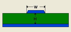
Again regarding the RF routing normally we go for 4 layer PCB. Trace impedance is very much dependant on the "distanve from the referance plane" in stripline routing, (refer picture) and it is difficult to control in two layer PCB.
Again do we need a complete ground plane for RF plane or we need it a good ground copper under the RF area?
69_1289636074.jpg
 

Status
Not open for further replies.

Part and Inventory Search

Welcome to EDABoard.com

Sponsor

Back
Top