Continue to Site

Welcome to EDAboard.com

Welcome to our site! EDAboard.com is an international Electronics Discussion Forum focused on EDA software, circuits, schematics, books, theory, papers, asic, pld, 8051, DSP, Network, RF, Analog Design, PCB, Service Manuals... and a whole lot more! To participate you need to register. Registration is free. Click here to register now.

Turn on waveform of power MOSFET

Status
Not open for further replies.

pastro

Junior Member level 3
Joined
Aug 20, 2010
Messages
25
Helped
0
Reputation
0
Reaction score
0
Trophy points
1,281
Activity points
1,538
Hi all,

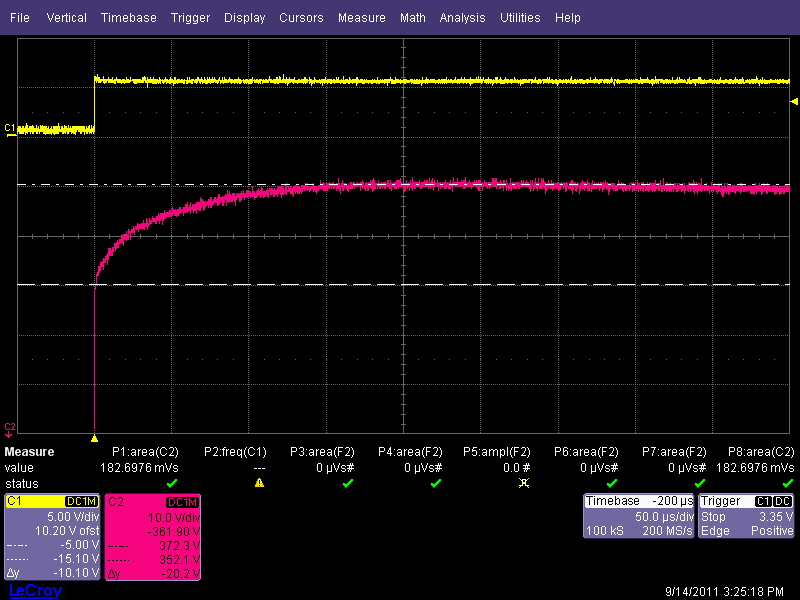
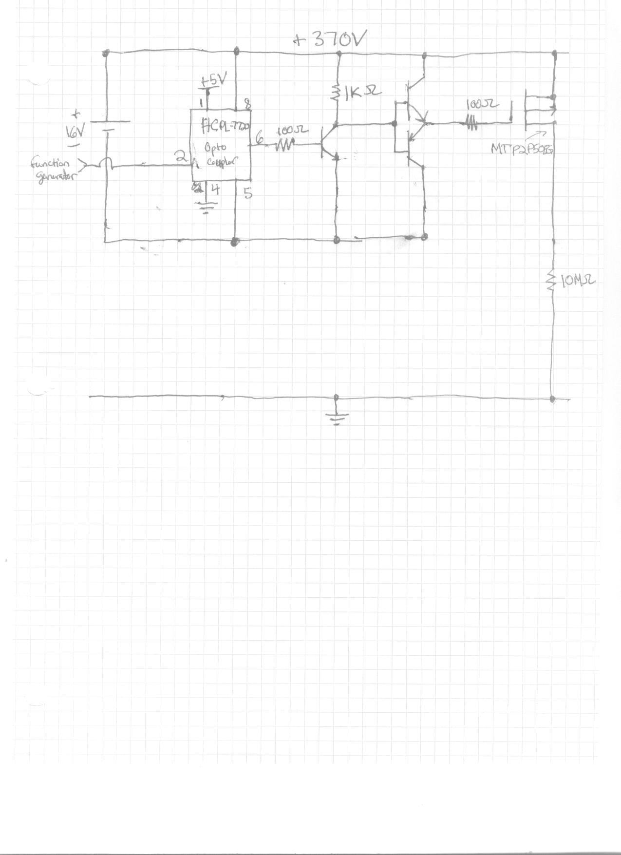
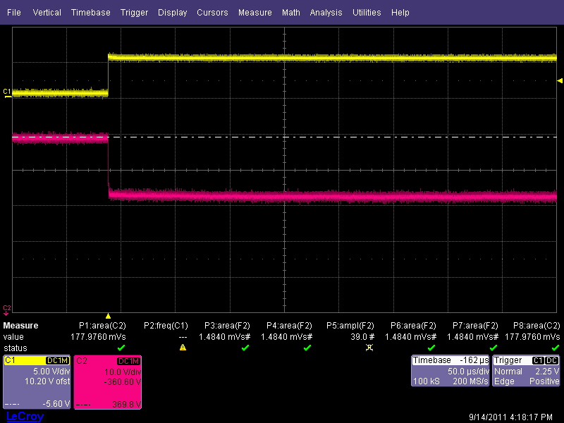
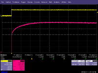
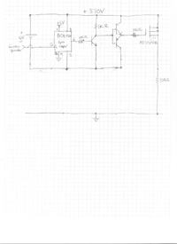
I'm using the MTP2P50EG P-Channel power MOSFET in order to attempt to switch a high voltage. I've prototyped the attached circuit, along with a scope screenshot of what I'm seeing at the output.

The trouble is that the waveform quickly shoots up to 350V in ~200ns, but then takes a long time to rise the extra 20V to 370V. My questions are 1.) Why does this happen? 2.) How to I fix it.

I need the waveform to shoot up to it's final voltage (370V) in this case, and stay there within ~500ns. In other words, I need much more square corners on the waveform.

Thanks!

Pastro


Are you sure that you checked the compensation of the HV probe? 40 uS time constant is a suspicious number in this regard.

"Every measurement is wrong" (unknown engineer)
 
  • Like
Reactions: pastro

    pastro

    Points: 2
    Helpful Answer Positive Rating
I'm using a 50MOhm high voltage prob for this. I checked with a squarewave, and the compensation looks fine.
 

What is your gate voltage waveform doing during this?
 
  • Like
Reactions: pastro

    pastro

    Points: 2
    Helpful Answer Positive Rating
I've attached the gate waveform


I see similar things in simulation, your DC I-V curve is
rolling over at that point (from constant-current to
constant-resistance). You might also have thermal-
spiked the device going through the high voltage *
high current region, degrading drive current until the
heat exits.

But then, your driver circuit shows no (370V-X) supply
connection. Are you sure the actual FET gate is well
driven (not the opto trigger)? Maybe it's not as solid
as you think. If this latter pic is the gate waveform,
it's the turnoff edge and shows nothing about the
original question.
 
  • Like
Reactions: pastro

    pastro

    Points: 2
    Helpful Answer Positive Rating
I'm not sure what is meant by a 370V-X connection. I'm using a battery to generate the 16V below 370V I show. (I'll use a DC-DC flyback converter later)

The pic I posted is the P-Channel MOSFET's gate waveform. Notice this is a P-Channel MOSFET, so a negative going edge is what you'd expect for turning on the device.
 

I've attached the gate waveform

Well that looks fine. I'd have to bet on some issue with either the probe or oscilloscope. I've had issues with some scopes before where if you try to look at waveforms with large offsets but low V/div (like viewing at 10mV/div with a common mode voltage of 5V), the scope simply won't acquire and display it correctly and I'll get weird waveforms like your. I've also seen such distortion coming from high voltage diff probes (from tektronix in particular). Usually it's due to excessive common mode voltage.

The circuit looks fine as drawn. Only thing that comes to mind is maybe the 370V is sagging during turn on, or maybe the resistor is drawing more current than you think (is it rated for 370Vdc?).
 
  • Like
Reactions: pastro

    pastro

    Points: 2
    Helpful Answer Positive Rating
I can still see this effect when the full voltage is on screen (At 50V/div) so I don't think it's the scope. This is the only HV probe I have, but I'll try dialing down the 370 to something more reasonable to see if I see similar effects on low voltage probes.

I showed the 10M there, but I still get this effect without that resistor, just using the input impedance of the HV probe connected to the MOSFET's drain. (50Mohms input impedance is stated). So I doubt it's the 10MOhm's voltage rating.
 

I don't see a reasonable explanation based on the shown circuit details. You can verify the measurement by replacing the transistor with a fast mechanical relay. Even a bouncing one should give a better edges. Ultimately, a mercury wetted relay could generate a sub-ns risetime reference pulse.
 
  • Like
Reactions: pastro

    pastro

    Points: 2
    Helpful Answer Positive Rating
Ah yes - thanks FVM - it is the turn on waveform, as the source rises there must be a dv/dt related current flowing through the gate drive (possibly all the way to the sig gen) which is keeping the Vgs in the threshold region and slowing the final part of the turn on. Try some CM chokes on the drive to the gate drive IC. Regards, Orson Cart.
 
Last edited:
  • Like
Reactions: pastro

    pastro

    Points: 2
    Helpful Answer Positive Rating
The answer is the RC time constant of the FET D-S capacitance and your load resistance - either the 10M res or the probe resistance or both. To turn OFF the mosfet has to charge up its D-S capacitance - if there is no low-ish impedance path for this to happen it will take a while to charge fully to rail. The output capacitance of a mosfet is also quite non-linear with voltage, which explains the shape of the waveform, with the C value increasing as the volts get closer to zero - slowing down the waveform more and more.... Regards, Orson Cart.

Look sharp. According to the schematic, it's a turn-on waveform. There is no obvious explanation for getting 40 us for 1/3 of the total step. Either the gate voltage is turning off again, the supply drops, or the measurement is wrong.
 
  • Like
Reactions: pastro

    pastro

    Points: 2
    Helpful Answer Positive Rating
Thanks to all for the excellent advice. I don't have any fast mechanical relays or CM chokes in the lab right now--I'll order them, but that will take a few days to come in. Otherwise, I don't think I have the ability to troubleshoot this any further, and there's other engineering to be done, so I've got to move on.
 

Can you confirm that the 370V is not sagging during the turn on?
 
  • Like
Reactions: pastro

    pastro

    Points: 2
    Helpful Answer Positive Rating
The 370V is definitely not sagging by more than 1V.

---------- Post added at 17:58 ---------- Previous post was at 17:55 ----------

There is no obvious explanation for getting 40 us for 1/3 of the total step. Either the gate voltage is turning off again, the supply drops, or the measurement is wrong.

Well, the gate voltage looks okay, I think (?). The supply definitely does not droop. So, by process of elimination, measurement error?
 

A mechanical switch or relay in place of (or parallel to ) the MOSFET can test the measurement setup.

The below waveform shows switching 80 V to a 1 Mohm 10:1 oscilloscope probe. You see contact bouncing (and minor overshoot caused by the setup), but the first edge is a clear step.


Status
Not open for further replies.

Similar threads

Part and Inventory Search

Welcome to EDABoard.com

Sponsor

Back
Top