funberry
Junior Member level 1
I am coming from 60Hz line transformer design, and somewhat new to SMPS.
I am trying to understand something about core saturation.
In laminated line trafo, the closest you ever come to saturation is during idle operation - no load on secondary, just magnetizing current.
Any current drawn from secondary will cause an increase in primary current, but that reflected current does not bring the core any closer to saturation, as it does not contribute net flux density ( in fact it brings you farther from saturation, by increasing copper losses.)
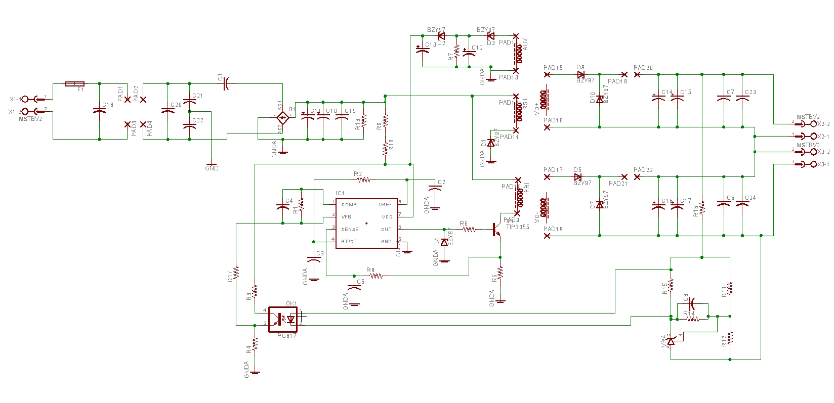
Is it the same in a single switch forward converter? The magnetizing current is the only contributor to net flux density?
Assume an open loop, where you peg the DC to 49% , then draw ever increasing current from the secondary ( ignoring for a moment copper losses). A naive thought would be that the ever increasing reflected primary current is converted into added flux, but that added flux is converted into secondary current, so no net flux density increase.
I have read that excessive load transients can sometimes cause saturation, and that would confirm that my understanding ( above ) is wrong.
So, can a FWD converter core saturate from secondary load, or are magnetizing current and duty cycle the only culprits?
thank you kindly.
I am trying to understand something about core saturation.
In laminated line trafo, the closest you ever come to saturation is during idle operation - no load on secondary, just magnetizing current.
Any current drawn from secondary will cause an increase in primary current, but that reflected current does not bring the core any closer to saturation, as it does not contribute net flux density ( in fact it brings you farther from saturation, by increasing copper losses.)
Is it the same in a single switch forward converter? The magnetizing current is the only contributor to net flux density?
Assume an open loop, where you peg the DC to 49% , then draw ever increasing current from the secondary ( ignoring for a moment copper losses). A naive thought would be that the ever increasing reflected primary current is converted into added flux, but that added flux is converted into secondary current, so no net flux density increase.
I have read that excessive load transients can sometimes cause saturation, and that would confirm that my understanding ( above ) is wrong.
So, can a FWD converter core saturate from secondary load, or are magnetizing current and duty cycle the only culprits?
thank you kindly.